CMPスラリーとは?CMPスラリー完全ガイド
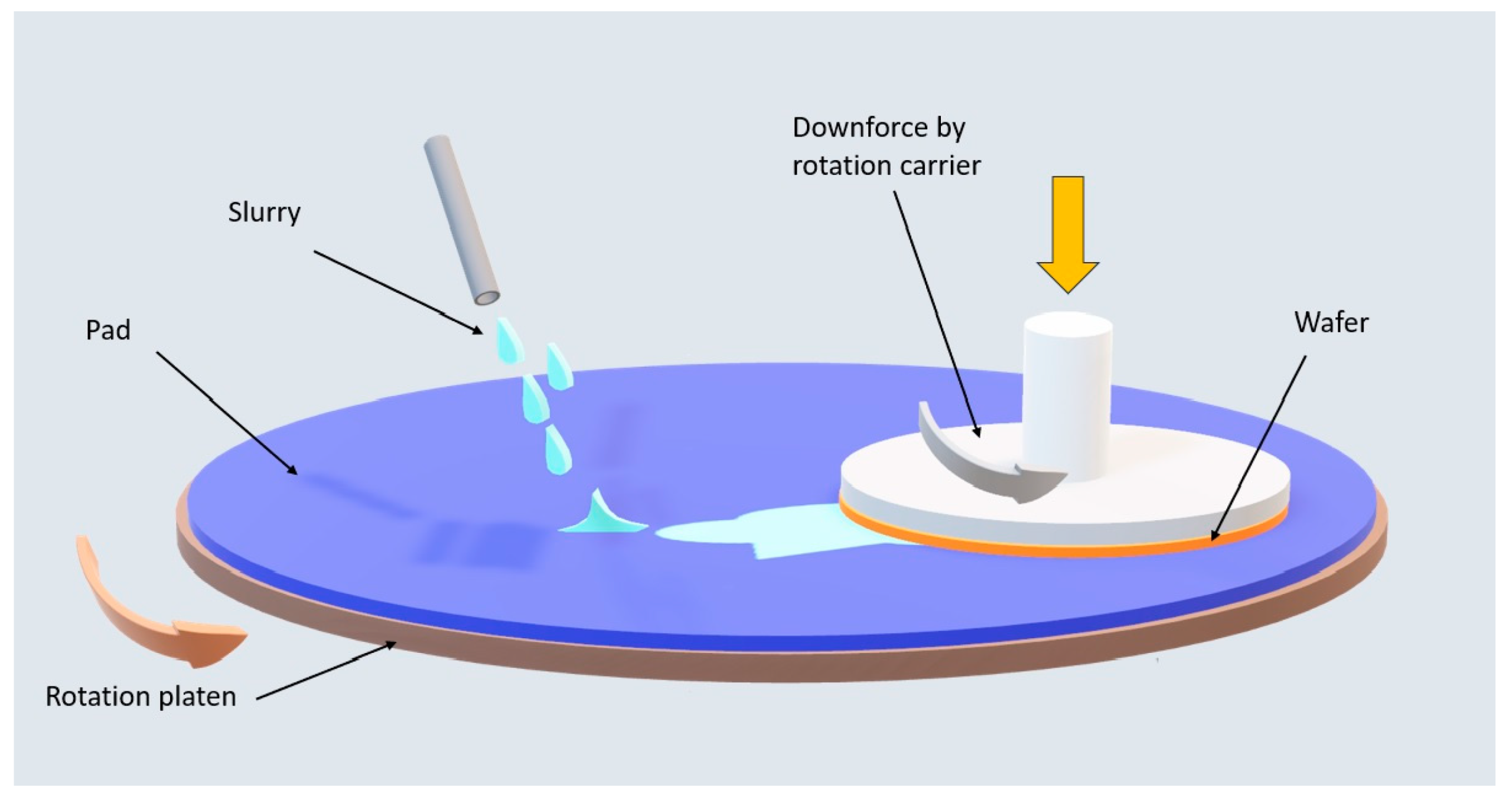
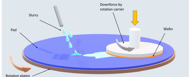
3nmノードのウェーハレベルの平坦化からチップレットの高度なパッケージングまで、CMPスラリーは現代の半導体製造を可能にする消耗品です。本ガイドは、CMPスラリーを使用するために必要なすべてを網羅しています。.
3nmノードのウェーハレベルの平坦化からチップレットの高度なパッケージングまで、CMPスラリーは現代の半導体製造を可能にする消耗品です。本ガイドは、CMPスラリーを使用するために必要なすべてを網羅しています。.
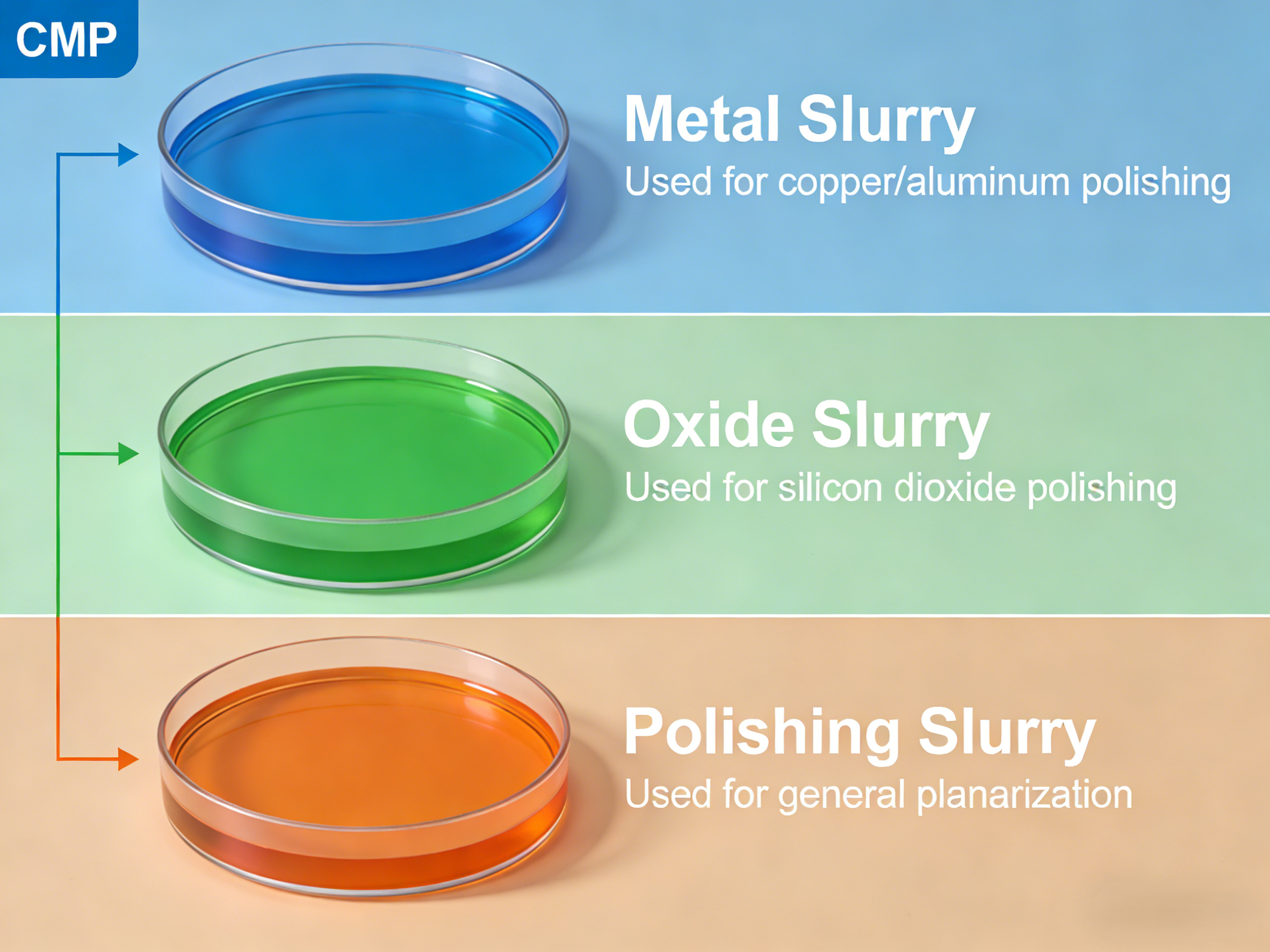
すべてのCMPスラリーが同じように作られるわけではありません。研磨剤の化学的性質、pH、選択性プロファイルが異なるためです。このガイドでは、半導体研磨の各工程で使用されるスラリーを ...
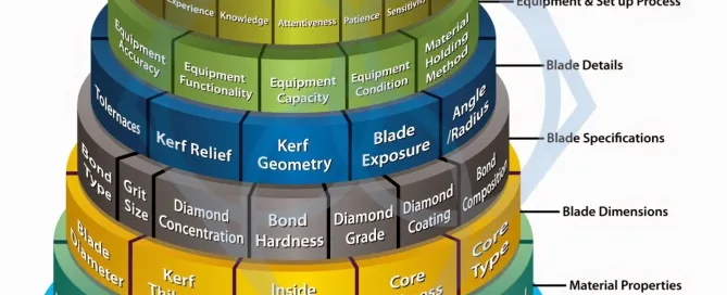
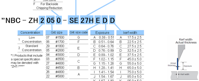
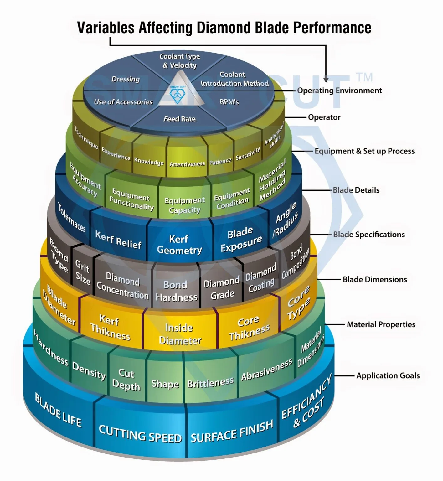
適切なダイシングブレードを選択することは、半導体ウェーハのシングレーションにおいて最も重要な技術的決定の一つです。多くの消耗品とは異なり、ダイシングブレードは、カーフロス、ダイエッジの品質、...
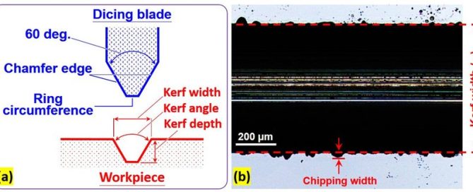
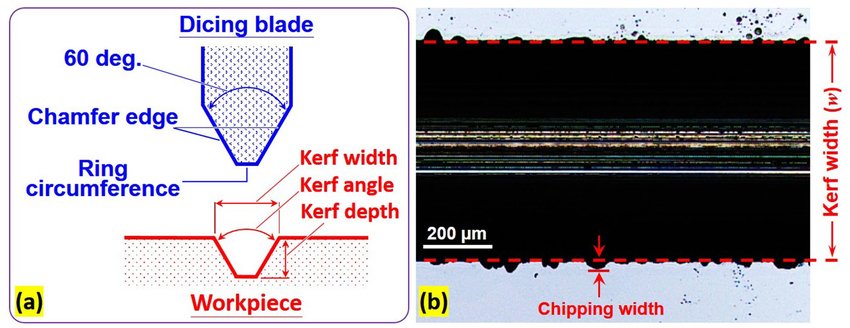
Dicing saw blade width is a critical parameter that directly determines kerf control, cutting precision, and blade path stability during wafer dicing. Although blade width is often discussed together with ...
Dicing saw blade thickness is one of the most critical yet frequently misunderstood parameters in wafer dicing. Blade thickness directly determines kerf loss, influences die mechanical strength, and must remain ...
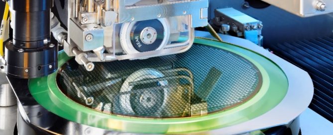
In semiconductor wafer singulation, the performance of diamond dicing blades is inseparable from the characteristics of the dicing equipment. Even a well-designed blade will fail to deliver stable cutting results ...
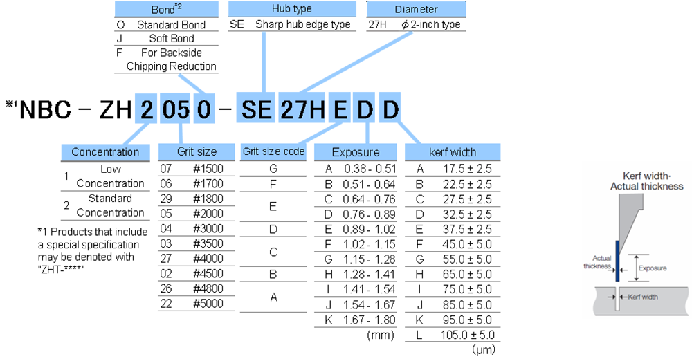
Accurate specification of dicing blades is a critical factor in semiconductor wafer singulation. Beyond nominal thickness and width, the interplay between diamond grit, concentration, bond type, equipment limits, and wafer ...
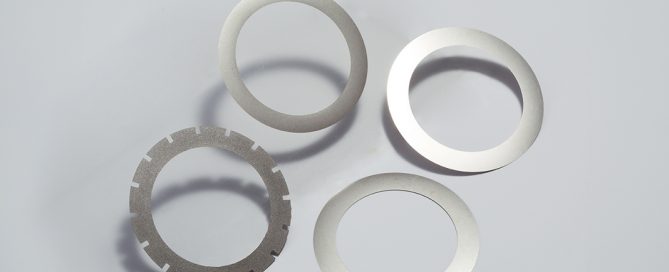
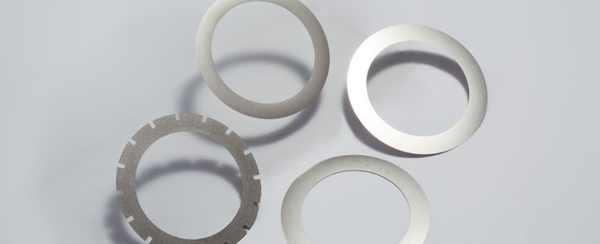
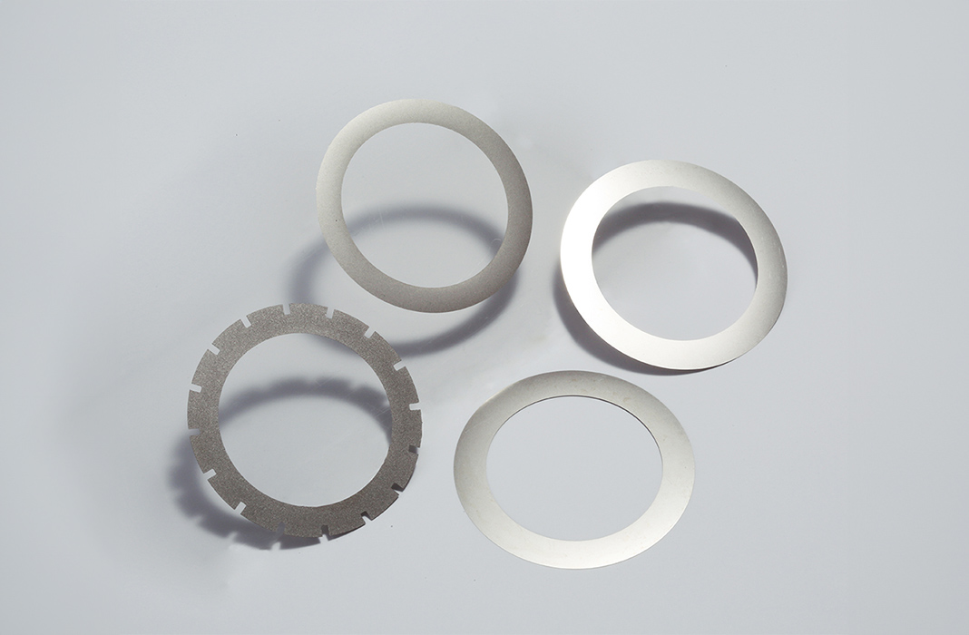
Diamond dicing blades for wafers are not generic cutting tools; they are highly engineered consumables designed to meet the mechanical, thermal, and material-specific requirements of semiconductor wafer singulation. As wafer ...
Diamond dicing blades are the core cutting tools used in modern semiconductor wafer singulation. From a product engineering perspective, a diamond dicing blade is not a generic consumable but a ...
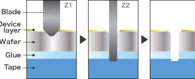
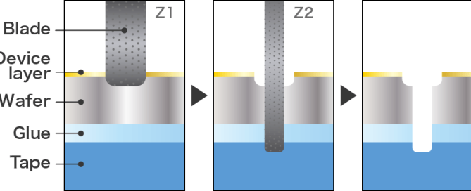
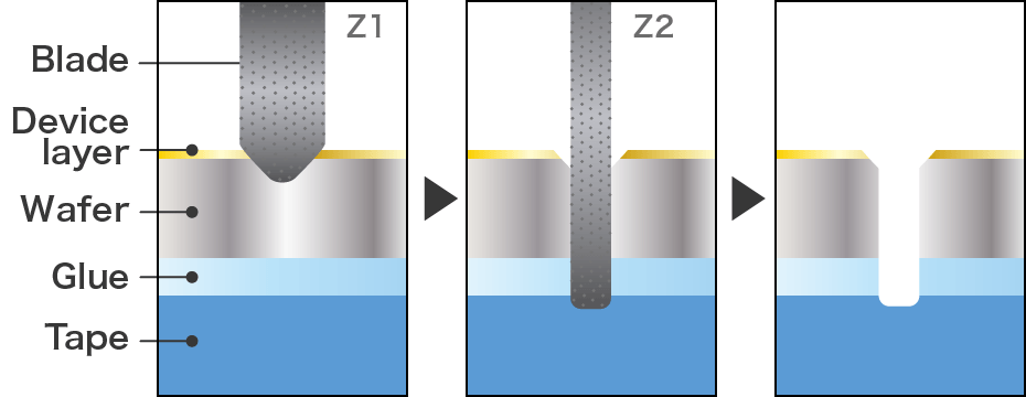
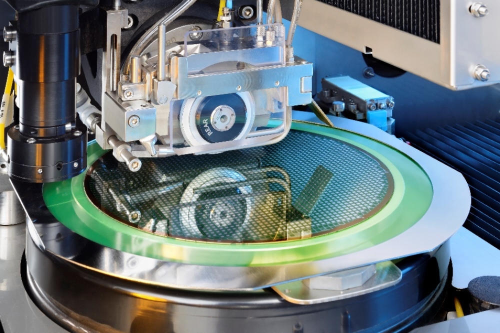
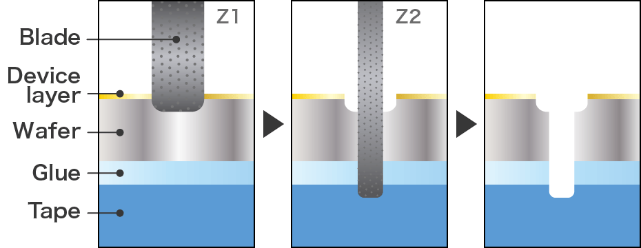
The blade dicing process is the most widely adopted wafer singulation method in semiconductor manufacturing. Despite the emergence of alternative technologies such as laser dicing and stealth dicing, blade dicing ...

高精度表面処理材料
ポリッシングスラリー - ポリッシングパッド - 半導体用ダイシングブレード
重要な製造工程における信頼性と一貫性。.
著作権 ©2026 無錫吉芝電子科技有限公司.

電話
+(86) 180-6835-1533

電子メール
contact@jeez-semicon.com

住所
中国江蘇省無錫市