CMP in Advanced Nodes:Challenges at 7nm, 5nm & Beyond
A detailed technical analysis of how CMP requirements evolve at leading-edge logic nodes — covering new device architectures (GAA, CFET), new interconnect materials (cobalt, ruthenium), ultra-low-k dielectric challenges, tightening metrology requirements, and the role of CMP in 3D NAND and advanced packaging through 2026 and beyond.
Why CMP Gets Harder at Each Node
Every technology node transition imposes stricter requirements on CMP across four dimensions simultaneously: tighter thickness targets, new materials with unfamiliar chemistries, more fragile film structures that cannot tolerate conventional polishing forces, and higher step counts that multiply the impact of any single-step imperfection on final yield. Understanding why these demands intensify with scaling is essential for anticipating where CMP process development resources must be focused.
This article extends the foundational CMP discussion in the CMP Semiconductor Complete Guide into the specific challenges encountered at 7 nm, 5 nm, 3 nm, and sub-3 nm process nodes. For a comparison of CMP process types across different film materials, see Copper CMP vs Tungsten CMP vs Oxide CMP.
Node-by-Node CMP Requirements
GAA & CFET: New CMP Steps
The transition from FinFET to Gate-All-Around (GAA) nanosheet transistors — commercialised by Samsung at 3 nm in 2022 and by TSMC and Intel at 2 nm in 2025 — introduces entirely new CMP process modules that have no precedent in previous-generation manufacturing.
SiGe Selective CMP for Nanosheet Release
GAA nanosheets are formed by depositing alternating layers of silicon (Si) and silicon germanium (SiGe) — typically 4–6 bilayers — and then selectively removing the SiGe layers to release the silicon nanosheets that form the transistor channels. One approach to nanosheet formation involves a CMP step to planarize the epitaxial stack before the SiGe etch, requiring a slurry with extremely high SiGe-to-Si selectivity (ideally >20:1) to stop reliably on the top silicon layer without over-polishing into it.
This selectivity requirement drives the development of novel ceria-based slurries with surface-passivating additives that preferentially protect Si while aggressively removing SiGe. The thickness of each silicon nanosheet — as little as 5 nm — means that even a few angstroms of over-polish can degrade transistor performance and uniformity.
Gate Dielectric Planarization
After high-k gate dielectric deposition and gate metal fill, a CMP step planarizes the gate stack to expose the source/drain contact regions. At GAA geometries, the lateral spacing between adjacent nanosheets is 5–8 nm — making this one of the most topology-challenging CMP applications in the entire process flow. Within-die removal uniformity at this step directly determines transistor threshold voltage uniformity across the chip.
CFET Interlayer CMP
Complementary FET (CFET) architecture stacks an nFET transistor directly on top of a pFET by separating them with an ultra-thin dielectric isolation layer. The interlayer CMP that planarizes this isolation dielectric must achieve height uniformity within 1–2 Å across the die to ensure that the upper nFET nanosheet stack is fabricated on a surface indistinguishable from a pristine substrate. This represents perhaps the most stringent CMP specification in the history of semiconductor manufacturing.
New Metals: Cobalt, Ruthenium & Beyond
The use of tungsten as the universal fill metal for contacts and local vias — a paradigm established in the 1990s — is being systematically displaced at advanced nodes by lower-resistance metals as line widths shrink below 20 nm and wire resistance becomes the dominant circuit performance bottleneck.
コバルトCMP
Cobalt was introduced for M0/V0 local interconnects at 10 nm and 7 nm nodes by Intel and TSMC. Unlike tungsten, cobalt has a significantly lower bulk resistivity (6.2 µΩ·cm vs 5.6 µΩ·cm for W, but with far lower barrier layer overhead at narrow widths), enabling lower contact resistance. However, cobalt CMP presents unique challenges that tungsten CMP does not:
- Cobalt is thermodynamically unstable in both acidic and strongly alkaline solutions — corroding readily — which severely constrains the accessible chemistry window for slurry design.
- Cobalt is prone to galvanic corrosion when in contact with copper or tungsten in the same CMP slurry environment.
- Cobalt ions (Co²⁺) in solution are cytotoxic and subject to strict environmental discharge limits — requiring dedicated wastewater treatment for cobalt CMP effluent.
- The optimal slurry pH for cobalt stability is approximately 8–9 — a narrow window that must be maintained within ±0.2 units throughout the slurry’s lifecycle.
ルテニウムCMP
Ruthenium is emerging as the preferred metal for both local interconnects (M0, M1) and metal gate fill at 2 nm and below. Its very low resistivity (7.1 µΩ·cm bulk, with superior scaling behavior at sub-5 nm line widths due to lower grain boundary and surface scattering) and good electromigration resistance make it attractive for the most critical wiring levels. Ruthenium CMP is even more challenging than cobalt: Ru is extremely hard and chemically inert in most acidic and alkaline solutions, requiring aggressive oxidisers (e.g., periodate, hypochlorite) to achieve practical removal rates. Slurry formulation for Ru CMP is an active area of research and development in 2026.
Ultra-Low-k Dielectric CMP
The progressive reduction of inter-metal dielectric (IMD) permittivity from SiO₂ (k = 3.9) through fluorinated silica glass (k = 3.5), to organosilicate glass (k ≈ 2.7), porous OSG (k ≈ 2.4), and now ultra-low-k porous dielectrics (k < 2.2) has been driven by the need to reduce RC delay in back-end interconnects. Each step down in dielectric constant is achieved by introducing porosity into the film — and each step down in k reduces the film’s mechanical strength and fracture toughness, making CMP progressively more challenging.
Delamination Risk
Porous ultra-low-k films with k values below 2.2 have elastic moduli below 5 GPa — compared to 70 GPa for SiO₂ — and critical adhesion energies (Gc) as low as 1 J/m². The shear stress applied during CMP polishing can exceed this adhesion energy at conventional polishing conditions, causing catastrophic film delamination at the dielectric-barrier interface. Preventing delamination requires reducing downforce, using softer pads with lower shear stress, and reformulating slurries with lower abrasive loading and improved surfactant packages that reduce the coefficient of friction at the polishing interface.
Moisture Absorption
Porous low-k films are highly susceptible to moisture absorption from aqueous CMP slurries. Water molecules that penetrate the pore network increase the effective dielectric constant of the film — partially negating the benefit of low-k — and can cause delayed delamination through hydrolysis of Si–C bonds at the film surface. Post-CMP low-k films therefore require a dedicated UV or thermal “cure” step to restore the dielectric properties and expel absorbed moisture before the next deposition step.
Metrology & Process Control at Scale
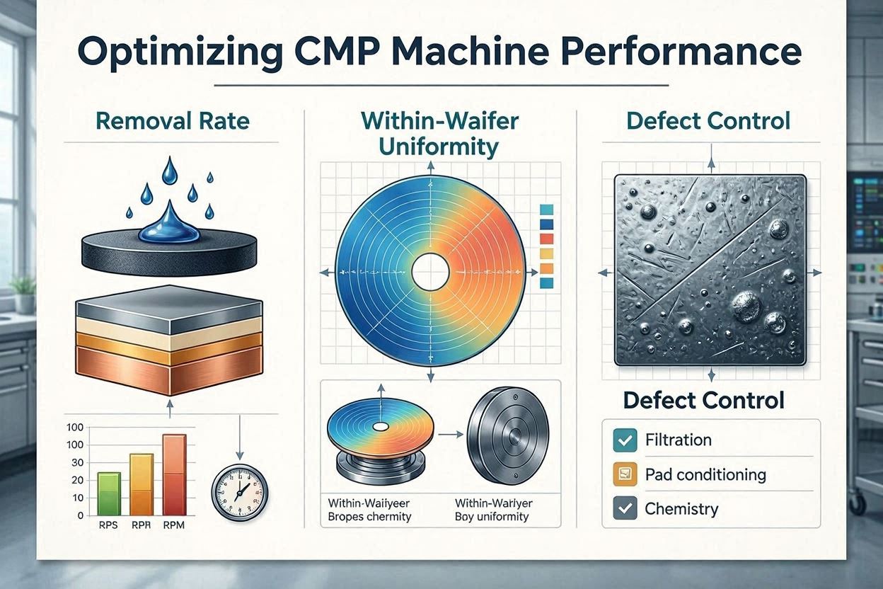
The tightening uniformity requirements at advanced nodes demand a corresponding evolution in in-situ and ex-situ metrology capability. The 1 nm WIWNU targets achievable at 7 nm must shrink to 0.3–0.5 nm at 3 nm and below — a standard that challenges the resolution limit of many commercially deployed metrology tools.
Broadband Reflectometry
Multi-wavelength optical endpoint detection provides real-time thickness mapping at multiple radial positions, enabling closed-loop pressure zone adjustment during polish.
Scatterometry (OCD)
Optical critical dimension scatterometry measures post-CMP surface topography with sub-nanometre sensitivity — increasingly used for advanced-node process qualification.
Eddy Current Metrology
Non-contact eddy current sensors measure metal film thickness in situ without requiring a pad window — used for copper and cobalt CMP endpoint and uniformity control.
Machine Learning APC
Advanced process control (APC) systems using machine learning models predict and correct for run-to-run thickness variation using feed-forward data from upstream deposition tools.
CMP in 3D NAND Flash
Three-dimensional NAND flash memory — the dominant storage technology in smartphones, SSDs, and data centres — relies on CMP throughout its fabrication but with a set of challenges distinctly different from logic CMP. In 2026, leading 3D NAND manufacturers including Samsung, SK Hynix, Micron, and Kioxia have reached 300+ layer stack heights, and the demands this places on CMP are extraordinary.
The core challenge is the sheer thickness of the oxide-nitride (ON) multilayer stack: at 300 layers, the total stack height exceeds 10 µm. CMP is used to planarize this stack after deposition and before staircase formation and channel hole etching. Polishing a 10 µm oxide film to nanometre-level uniformity across a 300 mm wafer requires slurries and pads optimised for high removal rate stability over very long polish times, and endpoint systems capable of detecting the transition from oxide to the underlying layer at the base of the stack.
Advanced Packaging & Hybrid Bonding
Perhaps the most transformative application of CMP in 2026 is its role in advanced packaging — specifically hybrid bonding, the technique that enables chiplets to be stacked face-to-face with sub-micron-pitch direct copper-to-copper interconnects. This application demands CMP performance that exceeds even the most demanding front-end logic requirements.
In hybrid bonding, copper bond pads and the surrounding dielectric (typically SiCN or SiO₂) must be co-planar within 1–2 nm, and the surface roughness must be below 0.3 nm Ra. Any step height between the copper pads and the dielectric — whether positive (proud copper) or negative (recessed copper) — creates a void at the bonding interface that reduces bond strength and electrical conductivity. Achieving this specification requires:
- Ultra-gentle CMP with downforce below 1 psi to avoid copper dishing
- Slurries specifically formulated for near-zero copper dishing — with carefully balanced corrosion inhibitor concentration
- Soft polishing pads that conform to local topography without introducing global non-uniformity
- Advanced in-situ metrology to detect sub-nanometre copper recess in real time
- A dedicated post-CMP cleaning step producing surface metal contamination below instrument detection limits
For the full discussion of CMP in 3D IC and heterogeneous integration, see our dedicated article: CMP in 3D IC & Heterogeneous Integration: New Frontiers.
Technology Outlook to 2030
Looking ahead from May 2026, the CMP technology roadmap through 2030 is shaped by four converging trends: continued transistor scaling toward 1.4 nm and angstrom-class nodes; proliferation of 3D integration and chiplet architectures; introduction of novel channel and interconnect materials (2D materials, topological metals); and the growing importance of compound semiconductor (SiC, GaN) CMP for power and RF applications.
Key CMP trends to watch through 2030
Atomic-layer CMP (ALCMP): Combining atomic-layer deposition (ALD) with CMP in a self-limiting planarization cycle for atomic-precision material removal.
2D material CMP: MoS₂, WSe₂, and other transition metal dichalcogenides (TMDs) as channel materials require CMP stop layers with atomic-monolayer precision.
AI-driven slurry development: Machine learning models trained on large CMP process datasets are accelerating slurry and pad formulation development cycles from years to months.
SiC and GaN CMP growth: The power electronics boom is driving rapid growth in SiC and GaN wafer CMP — a segment where conventional semiconductor slurry and pad suppliers are actively expanding capabilities.
CMP Consumables for Advanced-Node Applications
JEEZ supplies CMP slurries and polishing pads qualified for leading-edge applications. Our technical team supports process engineers at every node transition.
Contact JEEZ →