地子電子の最新動向、重要なお知らせ、企業ニュースなどをお知らせします。当社の成長の軌跡と重要なマイルストーンをお客様と共有することをお約束します。.
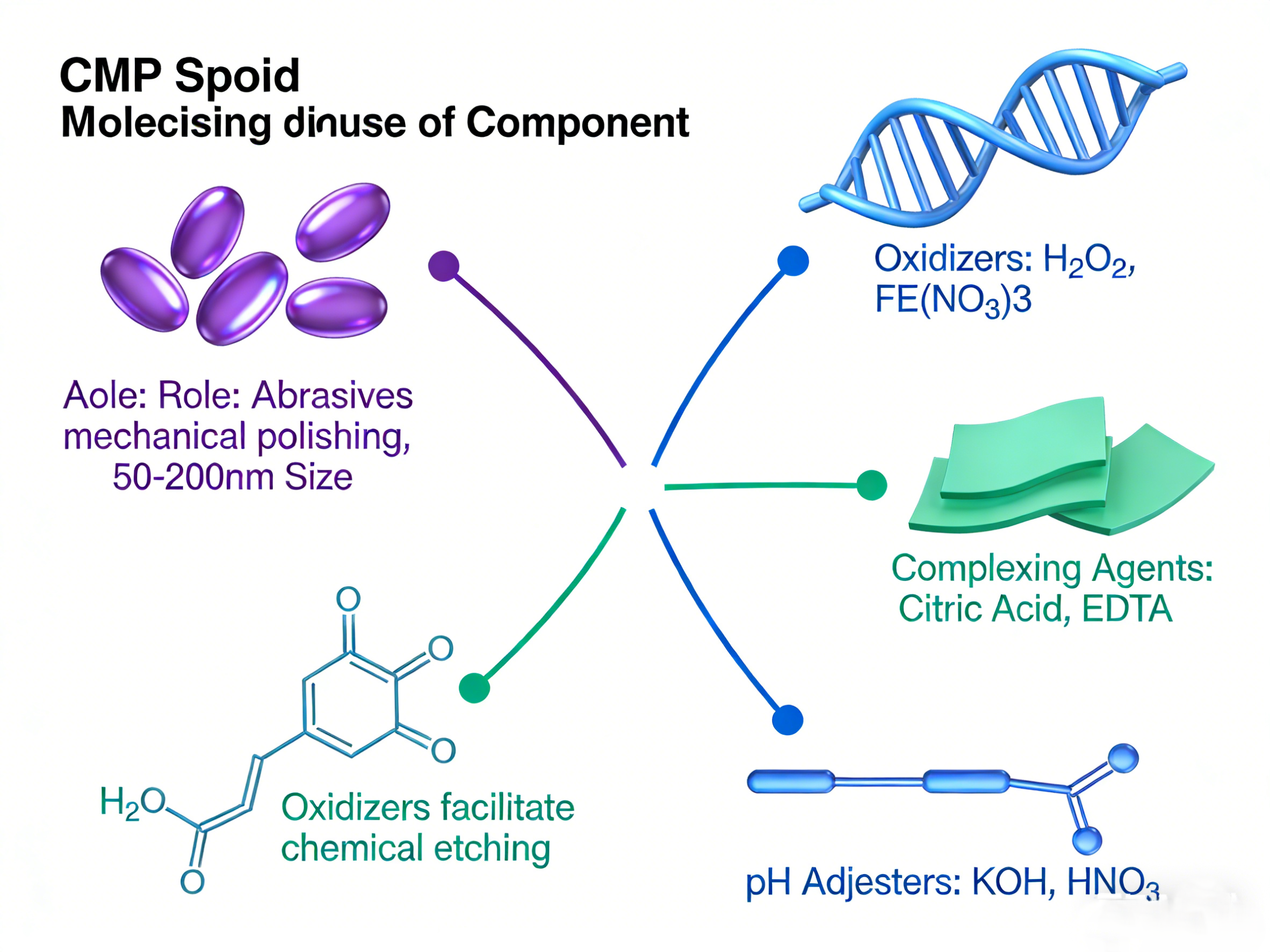
目次 1.はじめに 2.高レベル成分の概要 3. 研磨粒子 4.酸化剤と反応種 5.錯化剤とキレート剤 6.腐食防止剤と不動態化添加剤 7. pH緩衝剤とイオン制御 8.界面活性剤・分散剤 9.安定剤・保存料 10.微量不純物と汚染リスク 11.成分の相互作用と結合効果 12.成分の不均衡が引き起こす欠陥メカニズム 13.エンジニアリング・サマリー 1.はじめに 化学的機械的平坦化(CMP)において、スラリーは単純な研磨液ではない。スラリーは、機械的研磨、化学反応、界面輸送が正確なバランスを保たなければならない、注意深く設計された多相系である。 ...

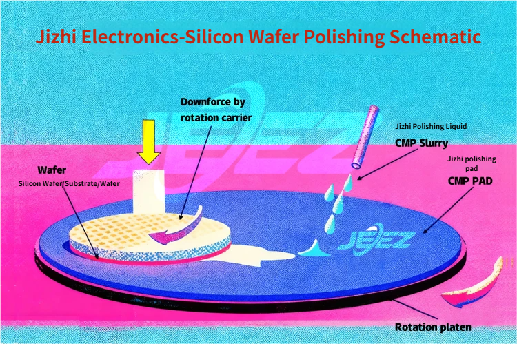
目次 はじめに CMPスラリーの基本的な構造 CMPスラリー中の砥粒 化学添加剤と酸化剤 複合化剤と腐食抑制剤 pH制御と化学的安定性 スラリーの安定性、分散性、および貯蔵寿命 工学パラメータ表 実験データと性能範囲 CMPスラリー・プロセス・ウィンドウ分析 組成に関連する故障モード CMPエコシステムにおけるCMPスラリー組成 はじめに CMPスラリー組成は、半導体製造における化学的機械的平坦化プロセスの基本的な挙動を定義する。CMPはしばしば化学と力学のハイブリッドと表現されますが、この2つのメカニズムが半導体製造プロセスでどのように相互作用するかを最終的に支配するのは、スラリーの配合です。.
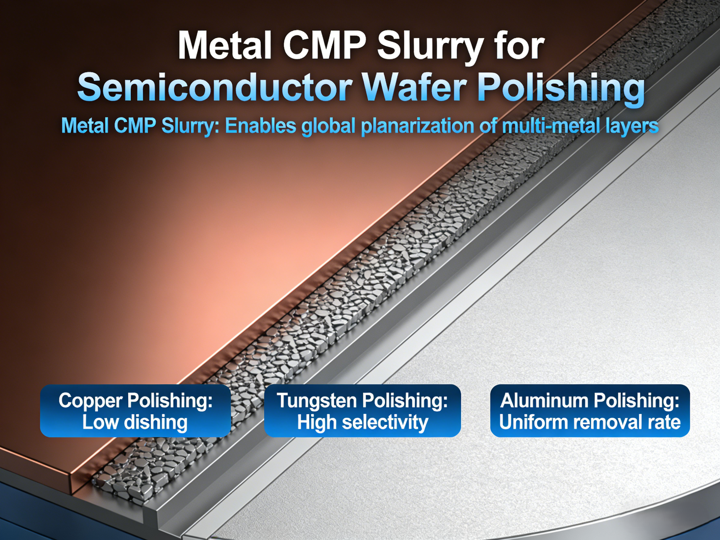
目次 1. メタルCMP入門 2. メタルCMPが根本的に異なる理由 3.メタルCMPスラリーの種類の分類 4.異なる金属間の除去メカニズム 5.メタルCMPスラリーの組成構造 6.金属特有のCMPスラリーに関する考察 7.エンジニアリングパラメーターと実験データ 8.プロセスウィンドウと統合制御 9.メタルCMPの欠陥と根本原因分析 10.大量生産の課題 11.メタルCMP用スラリー選択戦略 12.メタルCMPスラリーの将来動向 1.メタルCMPの紹介 メタルCMP(Chemical Mechanical Planarization)は、最先端半導体製造において最も重要な工程の一つです。半導体製造とは異なり ...
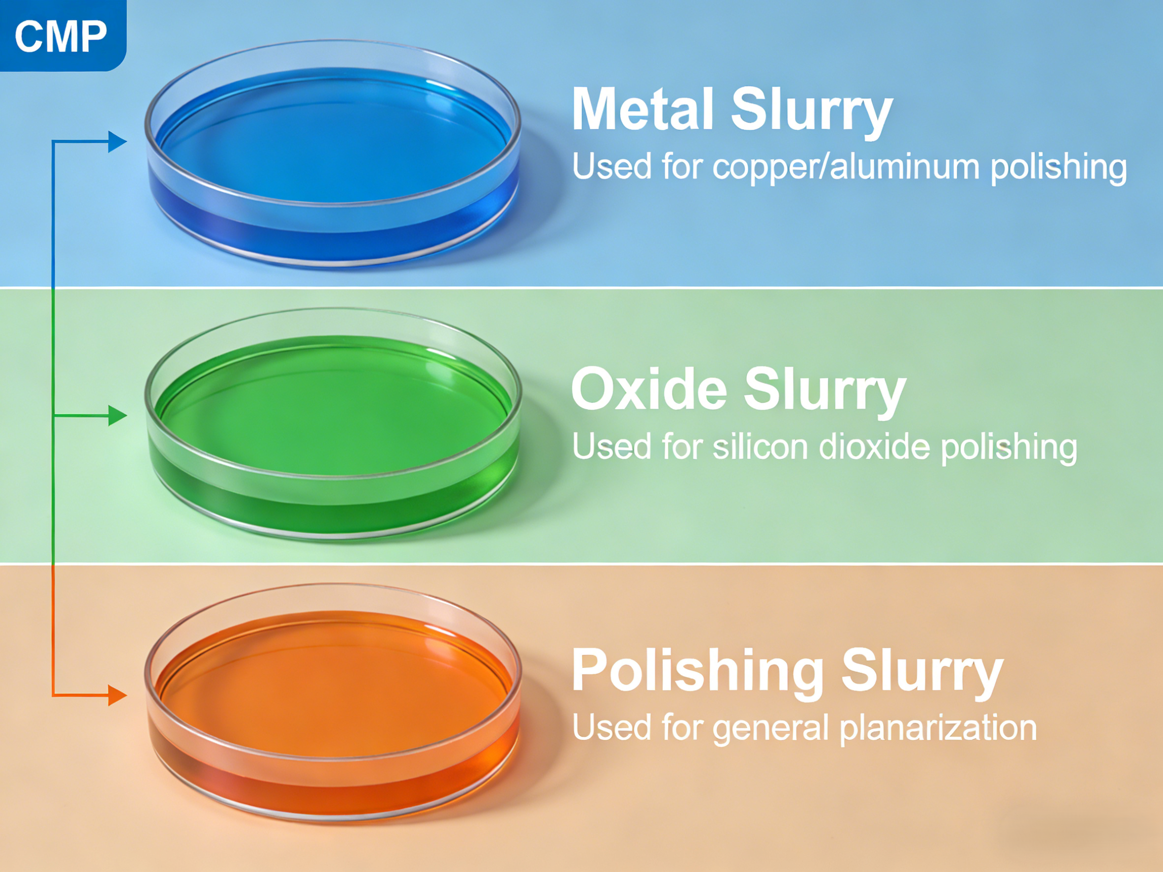
Table of Contents Introduction: Why CMP Slurry Types Matter CMP Slurry Classification Logic Oxide CMP Slurry Copper CMP Slurry Tungsten CMP Slurry Barrier & Hard Mask CMP Slurry Low-k & Advanced Dielectric Slurry Node-Driven Slurry Types Slurry Type vs Process Window Slurry Selection Decision Matrix Type-Specific Failure Modes Introduction: Why CMP Slurry Types Matter CMP slurry types are often oversimplified in commercial literature, frequently reduced to labels such as “oxide slurry” or “copper slurry.” In real semiconductor manufacturing environments, however, slurry type selection directly defines removal mechanisms, defect modes, integration risk, and ultimately yield. As technology nodes shrink and ...
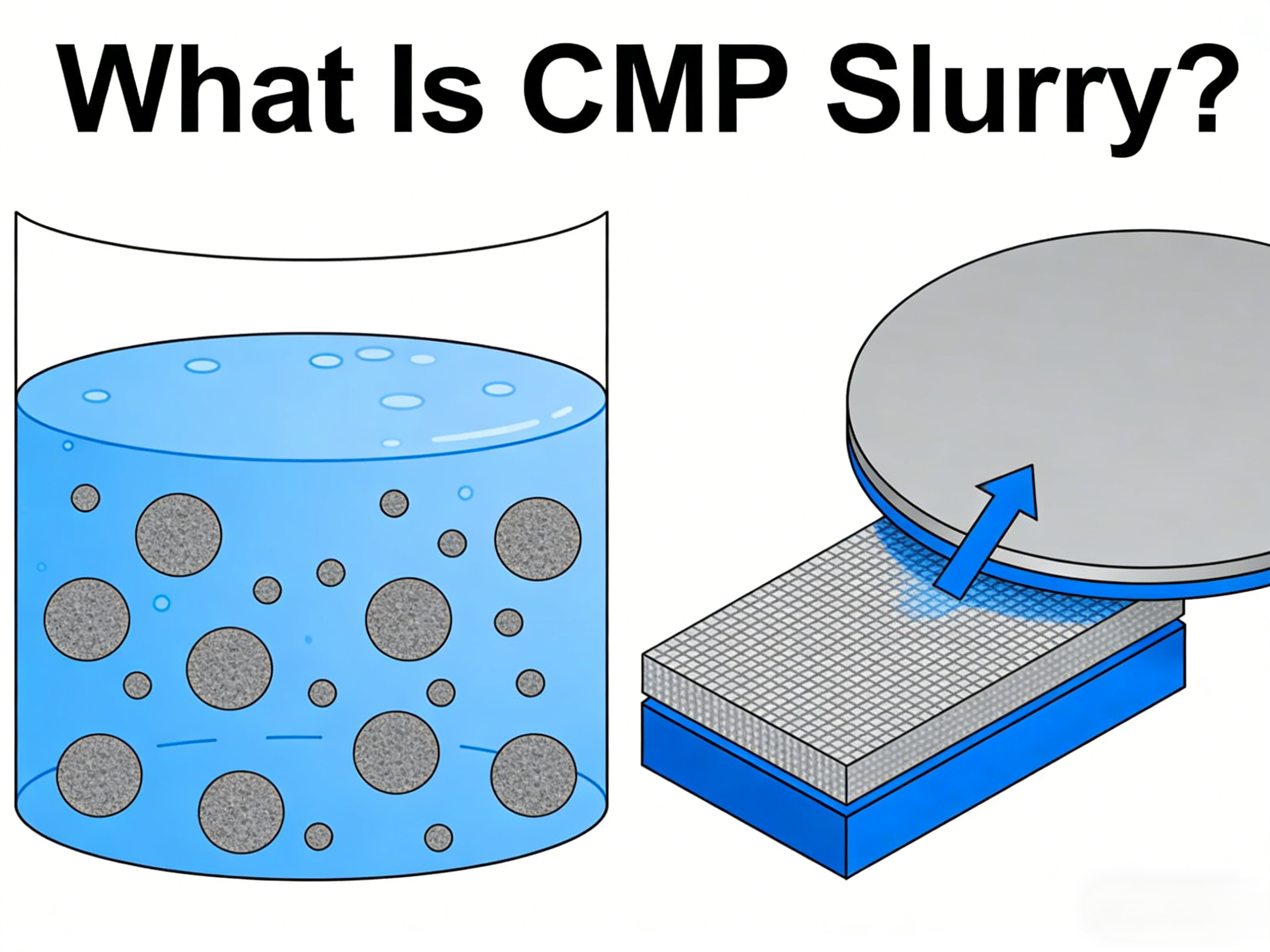
Table of Contents Definition of CMP Slurry CMP Slurry in Chemical Mechanical Planarization How CMP Slurry Works: Chemical and Mechanical Interaction Functions of CMP Slurry in Wafer Polishing Typical Applications of CMP Slurry CMP Slurry vs Conventional Polishing Compounds Key CMP Slurry Process Parameters Common Misunderstandings About CMP Slurry CMP Slurry Within the Complete CMP Ecosystem Definition of CMP Slurry CMP slurry is a chemically active, particle-based suspension specifically formulated for use in Chemical Mechanical Planarization (CMP) processes during semiconductor wafer manufacturing. Unlike generic abrasive slurries, CMP slurry is engineered to achieve highly controlled material removal through the combined ...
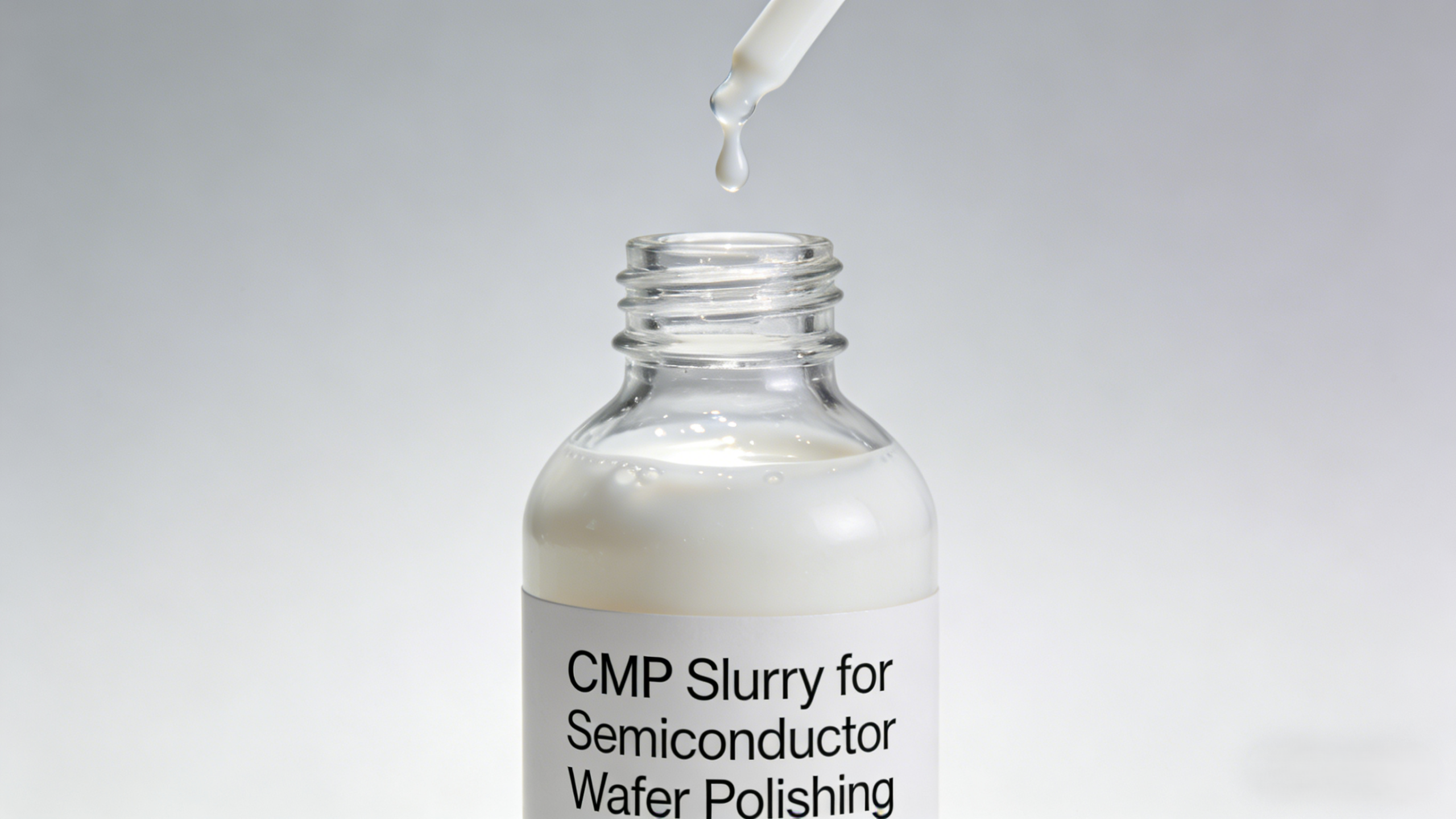
Table of Contents What Is CMP Slurry? Role of CMP Slurry in Semiconductor Manufacturing Types of CMP Slurry CMP Slurry Composition and Key Ingredients Metal CMP Slurry Applications CMP Slurry Filtration and Process Control How to Choose CMP Slurry for Wafer Polishing CMP Slurry Supplier and Custom Formulations What Is CMP Slurry? Chemical Mechanical Planarization (CMP) slurry is a highly engineered consumable used in semiconductor wafer polishing processes to achieve global and local planarization of thin films. Unlike conventional abrasive slurries used in mechanical polishing, CMP slurry is a chemically active suspension designed to interact with wafer materials at the ...
Indium Phosphide (InP), as a core material of the third-generation semiconductor, holds an irreplaceable position in high-end fields such as optical communications, millimeter-wave radar, and quantum communications due to its excellent electron mobility, wide bandgap, and superior optoelectronic properties. The surface quality of InP substrates directly determines the precision and reliability of subsequent epitaxial growth and device fabrication, with polishing and lapping processes being the critical steps in controlling this core metric. Drawing on years of practical experience in semiconductor material processing, Gizhi Electronics provides a systematic analysis of the key polishing and lapping processes for InP substrates, along with ...
In the precision manufacturing chain of the semiconductor industry, the creation of every high-performance chip relies on hundreds of process steps, from silicon purification to chip packaging. Among these, silicon wafer polishing—a critical process connecting wafer cutting and grinding with subsequent lithography and thin-film deposition—can be called the “art of surface finishing” in semiconductor manufacturing. It shapes the wafer surface with nanometer-level precision, directly determining the chip’s performance, reliability, and yield. As a company deeply rooted in the electronics field, Gizhi Electronics fully understands the core value of this process. This article will delve into the technical essence of silicon ...
第三世代半導体産業が加速する今日、炭化ケイ素(SiC)は、その優れた高温耐性と高い絶縁破壊電界強度により、新エネルギー自動車用パワーデバイスや高周波通信デバイスなどのハイエンド製造分野の技術的景観を再構築している。SiC加工において重要な工程であるCMP(Chemical Mechanical Polishing:化学的機械的研磨)は、その中核となる消耗品である研磨パッドの性能に大きく依存しており、完成したデバイスの精度と信頼性を直接左右する。長い間、日本のフジボウのG804W研磨パッドは、世界のSiC CMP分野で主流の選択肢の一つであった。.
CMPプロセスを解き明かす:光学部品加工の分野において、化学的機械研磨(CMP)は高精度の表面平坦化を実現する中核技術です。化学的腐食と機械的研磨の相乗効果により、光学ガラスの精密加工を実現します。CMPプロセスの本質は、化学的作用と機械的作用の相乗効果にある。研磨スラリーに含まれる化学試薬がまずガラス表面と反応し、除去しやすい軟化層を形成します。この化学的前処理により、その後の機械的研磨の基礎が築かれ、軟化層がガラス表面を傷つけることなく容易に除去できるようになります。.
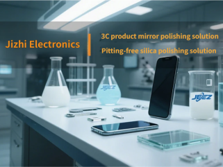
なぜ3C製品の鏡面研磨に電解研磨ではなくCMPを選ぶのか?3C産業(携帯電話、ノートパソコン、スマートウェアラブルなど)では、エッジのオーバーエッチングや材料の限界などの問題から、電気化学研磨は徐々にCMP(化学機械研磨)に取って代わられつつあります。ナノスケールSiO2研磨スラリーのメカノケミカルシナジーにより、Jizhi Electronicsは以下を実現します:表面粗さRa < 2nm、光学グレードミラーの要件を満たす。複雑な構造への適応性:複雑な構造への適応性:アルミニウム合金の中間フレームやステンレス製ボタンなどの不規則な部品に適しています。効率向上従来の方法に比べ、加工時間を30%短縮。シリカ研磨スラリーのピッティング問題を徹底分析 顧客から報告されたピッティング ...

半導体製造、精密光学、硬質合金加工などの分野では、材料表面の超精密研磨が製品の性能と信頼性を直接左右する。先進的な研究開発能力と成熟したプロセス技術を活用し、磁志電子は高性能のダイヤモンド研磨/研削スラリーシリーズを発表し、高硬度材料に効率的で安定した研磨ソリューションを提供する。Jizhi Electronicsのダイヤモンド懸濁液製品(研削スラリー/研磨スラリー)は、様々な研磨ニーズに対応し、材料特性とプロセス要件に基づいて以下のように分類されます:1.結晶構造による分類 単結晶ダイヤモンド研磨スラリー:単結晶ダイヤモンド研磨スラリー:単結晶ダイヤモンド研磨スラリーは、単結晶ダイヤモンドの結晶構造と均一な切削力を特徴とし、高精度の表面研磨と切削抵抗の低減に適している。.