Silicon Wafer Polishing Process: Step-by-Step from Lapping to Final Polish
A detailed technical walkthrough of every stage in the silicon wafer polishing sequence — lapping, chemical etching, double-side CMP, single-side finish CMP, and process control — with parameters, quality targets, and inter-stage quality dependencies.
Why the Polishing Sequence Is More Than the Sum of Its Steps
Silicon wafer polishing is a carefully sequenced chain in which each stage prepares the surface for the next — and in which mistakes propagate forward. Sub-surface crystal damage surviving the etch step will produce haze in CMP. Residual roughness from an under-conditioned DSP pad burdens the finish CMP step with excess material removal and increased defect risk. Understanding the physical purpose of each stage, the parameters that govern it, and the quality handoff criteria between stages is what separates a process engineer from someone who merely operates a tool.
This guide from Jizhi Electronic Technology Co., Ltd. (JEEZ) provides a detailed walkthrough of the complete silicon wafer polishing sequence from lapping through final inspection. It supplements our Complete Guide to Silicon Wafer Polishing, which covers the broader CMP landscape in a single reference article.
The Complete Polishing Sequence at a Glance
The path from a freshly sliced silicon disk to a polished, specification-compliant prime-grade wafer involves up to seven distinct stages. Each is necessary; none may be skipped without sacrificing downstream quality:
- Lapping Mechanically flatten both surfaces; remove bulk of slicing-induced waviness and establish initial TTV below 5 μm. Removes 30–60 μm per side.
- Edge Profiling Round wafer edges to the standardized chamfer profile (SEMI M1) using a diamond grinding wheel; prevents micro-cracking during subsequent handling and polishing.
- Chemical Etching Dissolve the sub-surface crystalline damage layer introduced by lapping. Acid etch (HF/HNO₃) removes 10–30 μm isotropically; alkaline etch (KOH) removes the same depth anisotropically along crystal planes.
- Double-Side CMP (DSP) Simultaneously polish front and back surfaces to achieve tight global flatness (TTV <1 μm, bow <40 μm) and reduce roughness to below 0.5 nm Ra. Removes 10–20 μm per side.
- Single-Side Finish CMP (SSP) Final ultra-low-removal-rate polish of the front surface. Removes only 0.5–1.5 μm but achieves Ra <0.1 nm, LPD <30, and haze <0.03 ppm.
- Post-CMP Cleaning Multi-step chemical cleaning (SC-1, SC-2, megasonic) removes all slurry residues, organics, and metallic contamination to sub-ppb levels.
- Metrology and Final Inspection TTV, SFQR, Ra, LPD, and haze measurements verify compliance with all specification limits before packaging and shipment.
Lapping: Mechanical Flatness Foundation
A rotary lapping machine uses a precision-flat cast iron or ceramic plate rotating at 20–60 rpm. The wafer is held in a carrier ring against the plate under 20–50 g/cm² load. A free-abrasive slurry of Al₂O₃ or SiC (3–20 μm grit) in a glycol-water carrier rolls between the plate and wafer in three-body abrasion, plastically fracturing and removing silicon at ~0.5–2 μm/min per side.
Lapping reduces TTV from the >20 μm typical of as-sliced wafers to below 3–5 μm, and corrects bow and warp to below 50 μm. However, the three-body abrasion mechanism leaves a sub-surface damage (SSD) layer 5–20 μm deep of fractured and plastically deformed silicon. This SSD layer must be completely removed by chemical etching before CMP, or crystalline defects will propagate into any epitaxial layers grown on the wafer.
Chemical Etching: Removing Sub-Surface Damage
Wet chemical etching removes the SSD layer from lapping by dissolving silicon without applying mechanical force. Two chemistries are in commercial use, each with distinct surface characteristics:
Acid Etch (HNA)
- HF + HNO₃ + CH₃COOH, room temperature
- Isotropic — uniform etch rate in all crystal directions
- Removes 10–30 μm per side
- Produces smooth, bright, rounded surface
- Generates NOₓ fumes — requires exhaust scrubbing
- Common for 150mm and specialty wafer grades
Alkaline Etch (KOH)
- 40–60 wt% KOH at 70–90°C
- Anisotropic — {111} planes etch ~100× slower than {100}
- Removes 10–30 μm per side
- Leaves micro-pyramidal surface texture on (100) wafers
- Introduces K⁺ contamination → thorough DI rinse required
- Standard for 300mm prime-grade production
The etch step’s most critical specification is completeness. An under-etched wafer retains residual crystal damage that manifests as elevated COP density or anomalous removal rate behavior in CMP. Etch depth is monitored by gravimetry (weight loss), with minimum removal set at 3× the estimated SSD depth. Over-etching is less harmful but wastes silicon and increases wafer taper risk in the etch bath.
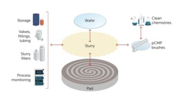
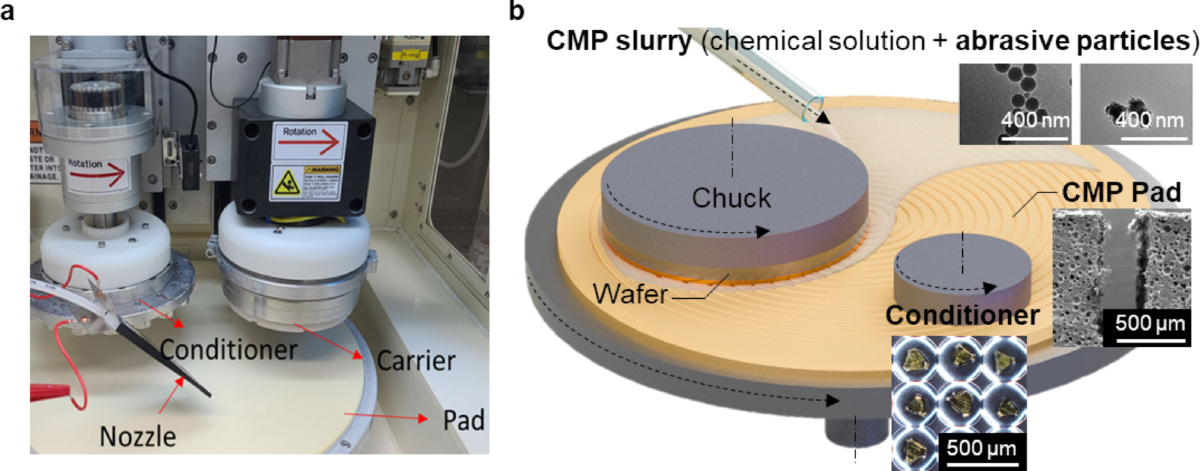
Double-Side CMP (DSP): Stock Removal and Precision Geometry
In a double-side polishing machine, the wafer rides freely in a thin, precision-machined carrier plate between upper and lower platens, each carrying a polishing pad. Because the wafer floats in the carrier plate’s hole under uniform pressure from both sides, it polishes simultaneously from top and bottom — and more importantly, its thicker regions receive higher contact pressure from both pads, driving the self-planarizing geometry correction that defines DSP’s strength.
Slurry: colloidal silica 80–150 nm D50, 5–15 wt%, pH 10.5–11.5. Pads: hard polyurethane (Shore D ~65). Applied pressure: 1.5–3.5 psi per side. Removal rate: 300–600 nm/min per side. Total removal: 10–20 μm per side.
DSP Output Quality Targets (300mm Prime)
| Метрика | Post-DSP Target | Controlled By |
|---|---|---|
| TTV | <1.0 μm | Carrier plate flatness, pad stiffness, pressure uniformity |
| Bow | <40 μm | Symmetric removal from both sides; carrier plate geometry |
| Warp | <60 μm | Same as bow |
| Front/back Ra | <0.5 nm | Slurry particle size, pad type, pH |
| Haze | <0.5 ppm | Slurry quality, rinse completeness |
For a deep comparison of DSP vs. SSP equipment, process architecture, and application selection, see: Single-Side vs. Double-Side Polishing: Which Is Right for Your Wafer?.
Single-Side Finish CMP (SSP): Delivering the Final Surface
The finish CMP step polishes only the front (device) surface. The wafer is held face-down on the carrier head membrane, which applies a very low, uniform pressure (0.5–1.0 psi / 3.5–7 kPa) against a rotating soft Suba-type pad. Slurry is fine colloidal silica (D50 20–50 nm, 0.1–2 wt%) or abrasive-free alkaline solution. Removal: 0.5–1.5 μm. Time: 10–30 min depending on slurry chemistry and pressure.
Chemical action — the formation and progressive removal of the silicic acid surface layer — dominates mechanical abrasion in this regime. The result is progressive smoothing of micro-asperities to below the atomic step level, elimination of haze, and reduction of the LPD count to specification. The SSP step cannot correct SFQR or TTV (removal is too shallow); those parameters are set in the DSP step and preserved here.
Process Control: Key Parameters and Monitoring
| Параметр | DSP Range | SSP Range | Effect of Deviation |
|---|---|---|---|
| Carrier/head pressure | 1.5–3.5 psi | 0.5–1.0 psi | High: elevated RR, scratch risk; Low: slow RR, possible uniformity issues |
| Platen rotation speed | 20–40 rpm | 30–60 rpm | Higher: faster RR; must stay within pad temperature budget |
| Slurry flow rate | 200–500 ml/min | 100–250 ml/min | Too low: starvation, non-uniformity; too high: waste |
| Slurry pH at tool inlet | 10.5–11.5 | 9.8–10.5 | Drift low: RR drop; drift high: haze, COP exposure risk |
| Pad temperature | 22–32°C | 20–28°C | Higher temp: faster chemical rate; lot-to-lot RR inconsistency if uncontrolled |
Post-CMP cleaning is the step that converts a polished wafer into a shippable substrate. For the full cleaning sequence and its role in final LPD performance, see: Post-CMP Cleaning for Silicon Wafers: Methods and Best Practices.
Часто задаваемые вопросы
Optimize Your Silicon Wafer Polishing Process with JEEZ
JEEZ supplies CMP slurries for every silicon wafer polishing stage and provides hands-on process consultation for recipe development, slurry stage-matching, and yield improvement on 200mm and 300mm production platforms.
Contact JEEZ Technical Team