Post-CMP Cleaning for Silicon Wafers: Methods and Best Practices
A complete technical guide to post-CMP cleaning — covering contamination types, SC-1 particle removal, SC-2 metal removal, DHF dip, megasonic cleaning, brush scrubbing, and Marangoni drying — with process parameters and LPD performance targets.
Why Post-CMP Cleaning Is a Process-Defining Step, Not a Clean-Up Step
The most common misconception in silicon wafer CMP operations is that post-process cleaning is simply a rinse to wash away polishing residue — a trivial step after the real engineering work of CMP is done. In reality, post-CMP cleaning is the step that determines whether the carefully optimized CMP process will translate into a wafer that passes final inspection. A polished surface with Ra = 0.08 nm and excellent SFQR will still fail inspection — and ultimately be rejected — if post-CMP cleaning leaves residual particles, organic films, or metallic contamination above specification.
This guide from Jizhi Electronic Technology Co., Ltd. (JEEZ) covers every major cleaning step in the post-CMP sequence, the contamination types each step removes, the process parameters that govern its effectiveness, and how to design an optimized cleaning sequence for your specific application. It is a companion to our broader Complete Guide to Silicon Wafer Polishing.
What Is Left on the Wafer Surface After CMP?
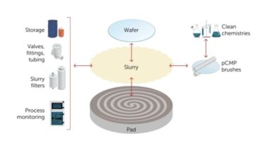
Immediately after the polishing step and before any cleaning, the silicon wafer front surface carries a complex mixture of at least four distinct contamination types, each requiring a different chemical approach for effective removal:
- Particulate contamination: Residual slurry abrasive particles (colloidal silica, 20–150 nm diameter) that have physically adsorbed to the polished silicon surface. Adhesion is primarily electrostatic: at typical post-polish pH values (9–10), the silicon surface carries a slight net charge that can attract or resist particle adhesion depending on the specific surface chemistry. Additional particles include polishing pad debris (polyurethane fragments), environmental contamination from the cleanroom air, and crystalline silicon fragments from the polishing reaction itself.
- Organic contamination: Slurry formulations typically contain non-ionic surfactants, chelating agents, and dispersant polymers to maintain abrasive stability and improve surface passivation. These organic additives adsorb onto the polished surface as a thin (~0.5–2 nm) organic film. Left in place, they would appear as organic contamination in subsequent thermal process steps (oxidation, epitaxy) and could impact gate dielectric interface quality.
- Metallic contamination: Ionic metal species — principally K⁺ and Na⁺ from the alkaline slurry base (KOH or TMAH), and transition metals (Fe, Cu, Ni, Cr) from polishing pad hardware, platen surfaces, and slurry delivery components — are present in the slurry liquid and can deposit on the silicon surface during polishing or during the post-polish immersion period. Even trace-level metallic contamination (ppb range) is unacceptable in gate oxide applications because Na⁺ and K⁺ diffuse through SiO₂ under bias, causing threshold voltage shift and long-term reliability degradation.
- Dissolved silicon species: The polishing reaction dissolves silicon as SiO₂·nH₂O (silicic acid). At the high alkaline pH of CMP, silicic acid remains soluble. However, as the wafer is rinsed and the pH drops toward neutral during cleaning, silicic acid can precipitate as amorphous silica micro-deposits on the wafer surface, appearing as LPDs on post-clean inspection. Careful pH management during the rinse steps prevents this re-deposition.
SC-1 Cleaning (APM): Particle and Organic Removal
SC-1 — named from the original RCA cleaning protocol — uses an ammonium peroxide mixture (APM) of ammonium hydroxide (NH₄OH), hydrogen peroxide (H₂O₂), and ultra-pure deionized water, typically in a 1:2:10 volume ratio at 65–80°C.
SC-1 Removal Mechanisms
- Particle removal: SC-1 mildly etches the silicon surface at ~0.5–1 nm per minute, “undercutting” adhered particles and liberating them from the surface. Simultaneously, the NH₄OH raises the surface pH to ~10, ensuring that both the silicon surface and colloidal silica particles carry strongly negative zeta potentials — creating electrostatic repulsion that keeps dislodged particles from re-adhering. The H₂O₂ provides an oxidizing environment that helps break down organic coatings that might anchor particles.
- Organic removal: H₂O₂ oxidatively degrades adsorbed organic films (surfactant residues, polymer dispersants) into smaller water-soluble fragments that are rinsed away. The combination of alkaline pH and peroxide is effective against most non-ionic and anionic organic contaminants used in CMP slurry formulations.
SC-1 Operating Conditions
| Параметр | Standard Range | Примечания |
|---|---|---|
| NH₄OH : H₂O₂ : H₂O ratio | 1:2:10 to 1:2:20 | More dilute ratios reduce etch rate; less effective for tenacious particles |
| Temperature | 65–80°C | Higher temperature: faster etch and organic decomposition; risk of ammonia evaporation |
| Immersion time | 5–10 min | Sufficient for particle removal; longer risks excessive Si etch and roughness increase |
| Megasonic frequency | 900 kHz – 1 MHz (when used) | Acoustic cavitation at wafer surface physically dislodges stubborn particles |
SC-2 Cleaning (HPM): Metallic Contamination Removal
SC-2 uses a hydrochloric peroxide mixture (HPM) of hydrochloric acid (HCl), hydrogen peroxide (H₂O₂), and ultra-pure DI water, typically at a 1:1:5 ratio and 70–80°C. SC-2 is specifically engineered for metallic contamination removal — the contamination type that is most damaging to gate oxide reliability but least visually apparent.
SC-2 Chemistry
HCl provides Cl⁻ ions that form stable chloride complexes with transition metals (FeCl₃, CuCl₂, NiCl₂) and alkali metals (KCl, NaCl). These metal chloride complexes are highly soluble in the acidic SC-2 solution and are efficiently removed from the silicon surface into the bulk solution. H₂O₂ provides an oxidizing environment that promotes metal oxide dissolution and maintains the silicon surface in a passivated (oxidized) state, preventing metal re-adsorption during the cleaning step.
SC-2 is critical for gate oxide applications where K⁺ and Na⁺ — the primary metallic contaminants from KOH-based CMP slurries — must be reduced below 1×10¹⁰ atoms/cm². TMAH-based slurries reduce the K⁺/Na⁺ challenge but do not eliminate the need for SC-2, because Fe and Cu from process hardware remain significant contamination sources.
DHF Dip: Native Oxide Removal and Surface Passivation
A dilute hydrofluoric acid (DHF) dip — typically 0.5–1.0% HF in ultra-pure DI water at room temperature for 30–60 seconds — etches the native silicon oxide (SiO₂) layer that grows on the silicon surface during SC-1 and SC-2 cleaning. The DHF dip is not always included in post-CMP cleaning sequences but is used in specific applications:
- Before SC-1, as a first step to strip any thick native oxide and liberate metallic contamination trapped at the oxide/silicon interface
- After SC-2, to produce a hydrogen-passivated (hydrophobic) silicon surface that is highly resistant to re-oxidation and metallic contamination adsorption for the brief period before the wafer is further processed
- As a pre-epi clean, to ensure the silicon substrate surface is oxide-free immediately before epitaxial silicon deposition
The hydrophobic silicon surface produced by DHF is also useful for detecting contamination: particles that land on a hydrophobic surface adhere less strongly than on a hydrophilic (oxidized) surface, and the surface dries more uniformly. However, a hydrophobic surface is more susceptible to hydrocarbon adsorption from the ambient, so exposure time between DHF clean and the next process step must be minimized.
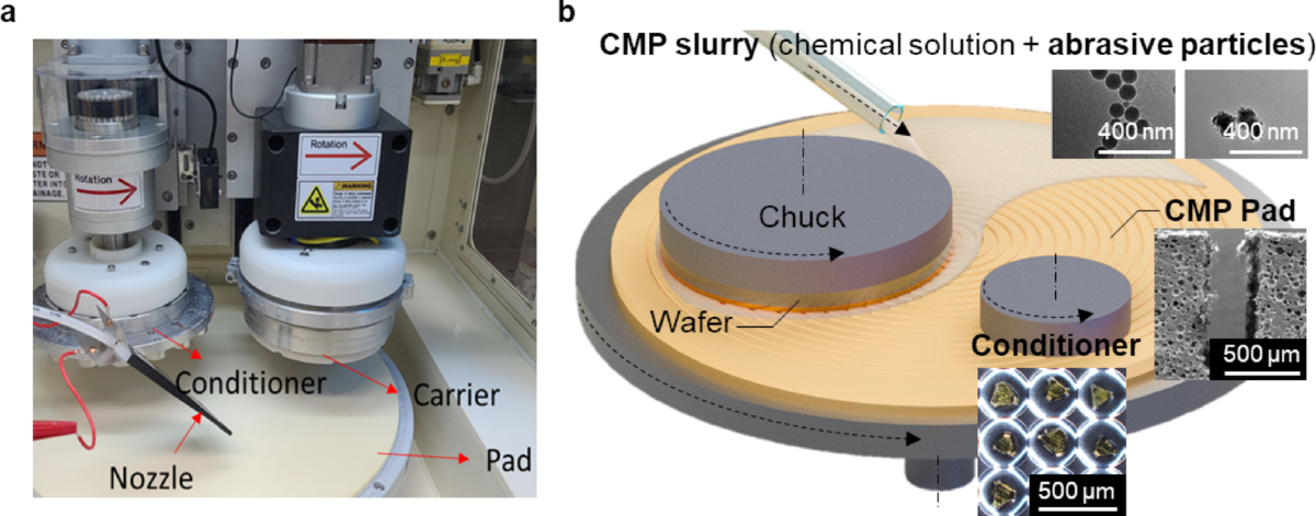
Megasonic Cleaning and Brush Scrubbing
Megasonic Cleaning
Megasonic transducers operating at 900 kHz–1 MHz are immersed in or mounted on the walls of cleaning baths to generate acoustic streaming and controlled micro-cavitation in the cleaning liquid. The resulting fluid motion at the wafer surface generates a boundary-layer shear stress that dislodges adhered particles too small to be removed by chemical mechanisms alone. Megasonic enhancement is particularly valuable for particles <100 nm, which have very high adhesion-to-removal-force ratios due to their large surface-area-to-mass ratio. The combination of megasonic energy with SC-1 chemistry is the most effective approach currently available for achieving LPD counts below 30 at 35 nm on 300mm prime silicon.
Brush Scrubbing (PVA Brush Clean)
Polyvinyl alcohol (PVA) sponge brush cleaners use rotating cylindrical brushes (100–300 rpm) that gently contact the wafer surface while ultra-pure DI water is dispensed. The brushes are sufficiently compliant to avoid surface scratching (contact force <0.1 N) while physically sweeping particles from the wafer surface. PVA brush scrubbing is effective for particles >100 nm and complements megasonic cleaning, which is more effective for smaller particles. Brush scrubbing is typically used as the first cleaning step after the polishing tool — before any chemical bath — to remove the bulk of slurry particles before the chemical steps refine the surface to specification.
Final Rinse and Drying: Preventing Watermarks
The final rinse uses ultra-pure DI water (resistivity >18.2 MΩ·cm, TOC <1 ppb, particle count <1 particle/ml at >50 nm) to dilute and flush all chemical residues from the SC-2 step to negligible levels. The rinse must be thorough enough that the last rinse water expelled from the wafer surface has a resistivity approaching that of the incoming DI water — typically monitored by an inline conductivity sensor in the overflow rinse tank drain.
Drying is where watermarks can be introduced. A water droplet that evaporates on the silicon surface concentrates its dissolved mineral load (silicic acid, trace metals, dissolved gases) into a ring-shaped deposit — a watermark — that appears as a cluster of LPDs at the evaporation boundary. Two drying approaches minimize watermarks:
- Spin-dry (centrifugal drying): The wafer is spun at 1,000–3,000 rpm in a N₂ ambient while a small volume of ultra-pure DI water is dispensed near the wafer center. Centrifugal force drives the water film uniformly off the wafer edge faster than it can evaporate from the surface, preventing stationary droplet formation. This is the most common drying method in 300mm post-CMP cleaning tools.
- Marangoni (IPA vapor) drying: The wafer is slowly withdrawn from the final DI water rinse through a zone of isopropyl alcohol (IPA) vapor. The surface-tension gradient (IPA has much lower surface tension than water) at the IPA/water interface drives the water film to retract from the wafer surface cleanly, without leaving droplets. Marangoni drying consistently delivers lower watermark density than spin-dry and is preferred for the most stringent LPD specifications.
For defect context on how incomplete cleaning manifests as LPD failures, see: Silicon Wafer Surface Defects in CMP: Causes, Detection & Prevention. For the complete process sequence that post-CMP cleaning follows, see: Silicon Wafer Polishing Process: Step-by-Step from Lapping to Final Polish.
Часто задаваемые вопросы
Cleaner Wafers Start with Cleaner Slurry
JEEZ CMP slurries are formulated with low organic additive loading and ultra-low metallic impurity levels (Fe, Cu <1 ppb), reducing the post-CMP contamination burden and making it easier to reach the LPD and metallic cleanliness targets your process requires.
Contact JEEZ Technical Team