logo

О semiconductor

Этот автор еще не указал никаких подробностей.
На данный момент semiconductor создал 195 записей в блоге.

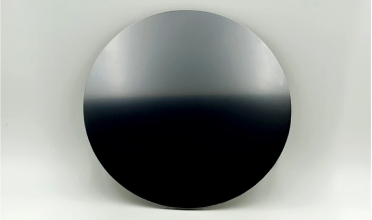
Шлам для полировки пластин из карбида кремния

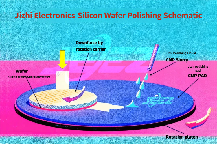
Gizhil Electronic's silicon carbide fine polishing slurry is suitable for the surface planarization of SiC silicon carbide wafer substrates during precision machining. The slurry used for wafer polishing exhibits high ...

По |2025-12-16T11:43:32+08:002025年12月9日|Приложение|Комментарии к записи Silicon Carbide Wafer Polishing Slurry отключены

Полировка твердых сплавов - зеркальная полировка лезвий из вольфрамовой стали

Hard alloy blades possess a series of excellent properties, including high hardness, good toughness, heat resistance, and corrosion resistance. Particularly, their high hardness and wear resistance allow them to maintain ...

По |2025-12-16T11:43:53+08:002025年12月9日|Приложение|Комментарии к записи Hard Alloy Polishing Slurry—Mirror Polishing of Tungsten Steel Blades отключены

Процесс полировки карбида кремния (SiC)

Depending on the specific semiconductor industry processes, CMP (Chemical Mechanical Polishing) slurries can be categorized into dielectric layer CMP slurries, barrier layer CMP slurries, copper CMP slurries, silicon CMP slurries, ...

По |2025-12-16T11:44:19+08:002025年12月9日|Приложение|Комментарии к записи Silicon Carbide (SiC) Polishing Process отключены

Анализ основных процессов полировки и притирки подложек InP (фосфида индия)

Indium Phosphide (InP), as a core material of the third-generation semiconductor, holds an irreplaceable position in high-end fields such as optical communications, millimeter-wave radar, and quantum communications due to its ...

По |2025-12-25T10:48:50+08:002025年12月5日|Блог, Промышленность|Комментарии к записи Analysis of Key Polishing and Lapping Processes for InP (Indium Phosphide) Substrates отключены

Поверхностная революция“ в производстве полупроводников: Техническая сущность и фундаментальная ценность полировки кремниевых пластин

In the precision manufacturing chain of the semiconductor industry, the creation of every high-performance chip relies on hundreds of process steps, from silicon purification to chip packaging. Among these, silicon ...

По |2025-12-05T11:01:27+08:002025年12月5日|Блог, Промышленность|Комментарии к записи The “Surface Revolution” in Semiconductor Manufacturing: The Technical Essence and Foundational Value of Silicon Wafer Polishing отключены

Преодоление высокой стоимости и медленного отклика G804W

As the third-generation semiconductor industry accelerates its iteration today, silicon carbide (SiC), as a core material, is reshaping the technological landscape of high-end manufacturing fields such as new energy vehicle ...

По |2025-12-05T10:57:18+08:002025年12月5日|Блог, Промышленность|Комментарии к записи Breaking Through the High Cost and Slow Response of G804W отключены

Раскрытие секретов использования полировальной суспензии для оптического стекла в процессах CMP

Unlocking CMP Process: Principles and Advantages In the field of optical component processing, Chemical Mechanical Polishing (CMP) is a core technology for achieving high-precision surface planarization. Through the synergistic effects ...

По |2025-12-05T10:50:44+08:002025年12月5日|Блог, Промышленность|Комментарии к записи Unlocking the Secrets of Optical Glass Polishing Slurry in CMP Processes отключены

3C Product Mirror Polishing Solution: Полировальная суспензия из кремнезема SiO2 без точечной коррозии

Why Choose CMP Over Electrochemical Polishing for 3C Product Mirror Polishing? In the 3C industry (mobile phones, laptops, smart wearables, etc.), electrochemical polishing is gradually being replaced by CMP (Chemical ...

По |2025-12-25T10:47:48+08:002025年12月5日|Блог, Динамика|Комментарии к записи 3C Product Mirror Polishing Solution: Pitting-Free SiO2 Silica Polishing Slurry отключены

Функции и эффективность алмазной подвески (специализированной для полировки CMP)

In fields such as semiconductor manufacturing, precision optics, and hard alloy processing, the ultra-precision polishing of material surfaces directly determines product performance and reliability. Leveraging advanced R&D capabilities and mature ...

По |2025-12-05T10:34:39+08:002025年12月5日|Блог, Динамика|Комментарии к записи Functions and Efficacy of Diamond Suspension (Specialized for CMP Polishing) отключены

Полировочный шлам CMP для электронных кремниевых пластин

I. Технология полировки CMP: Ключевой процесс в производстве полупроводников Химико-механическая планаризация (CMP) является одним из основных процессов в производстве полупроводниковых кремниевых пластин, непосредственно влияющим на производительность чипа и ...

По |2025-12-05T10:32:18+08:002025年12月5日|Блог, Динамика|Комментарии к записи CMP Polishing Slurry for Electronic Silicon Wafers отключены
Перейти к началу