logo

О semiconductor

Этот автор еще не указал никаких подробностей.
На данный момент semiconductor создал 51 записей в блоге.

Материалы и структура полировального коврика CMP объяснены

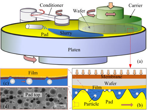
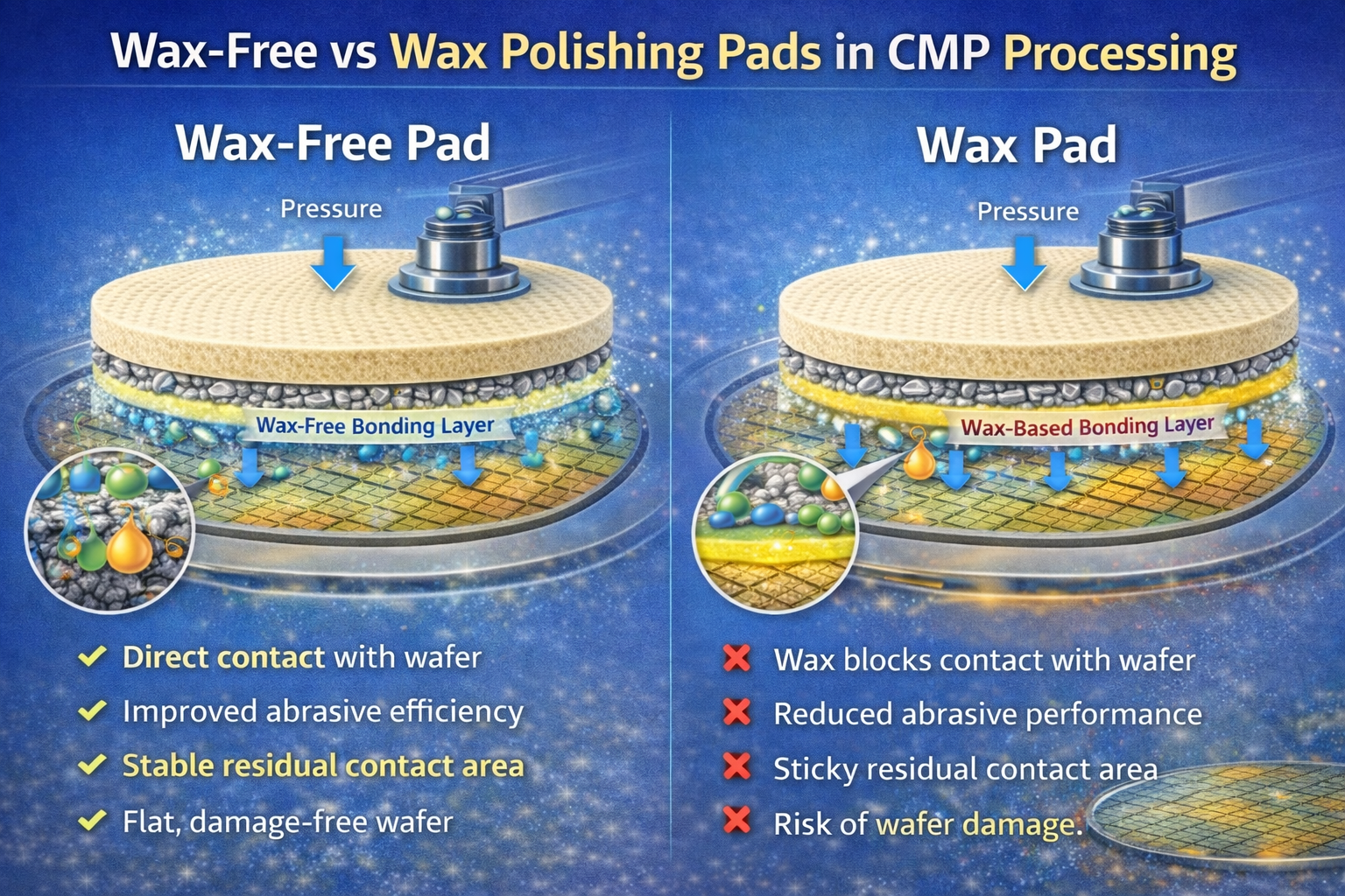
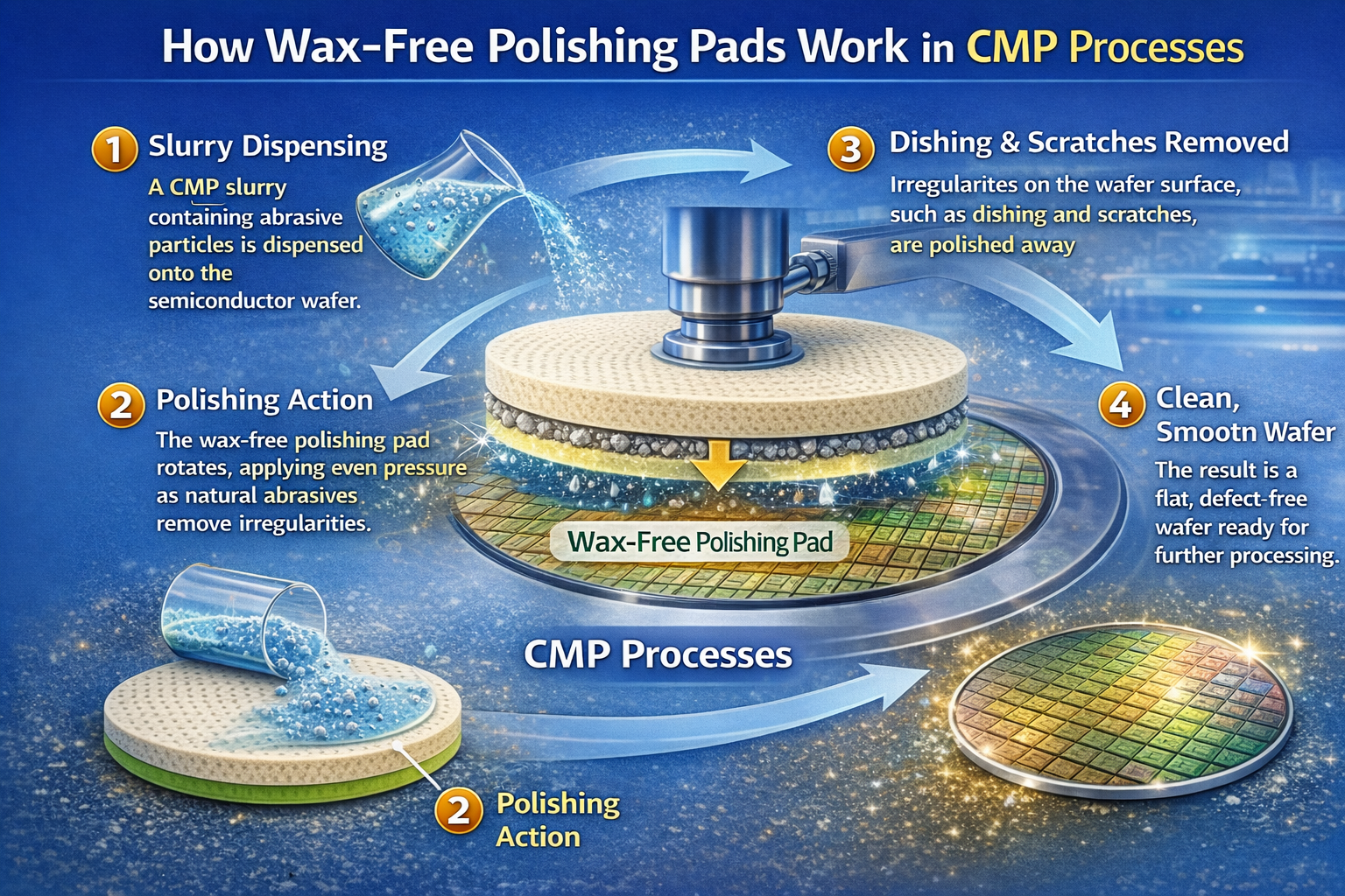
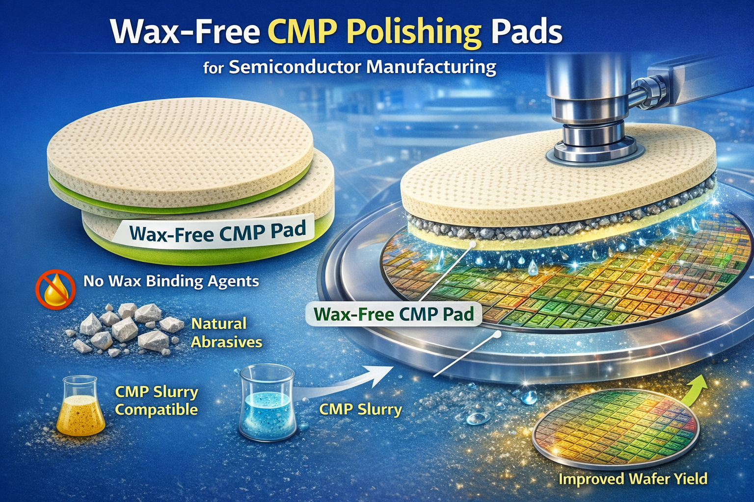
В CMP материалы полировальных подушек определяют фундаментальные механические, химические и трибологические взаимодействия, которые в конечном итоге определяют эффективность планаризации, дефектность и стабильность процесса. Для полировальных подушек CMP без воска выбор материала становится еще более критичным, поскольку фиксация пластин, передача усилия и взаимодействие со шламом определяются непосредственно свойствами основной массы и поверхности подушки, а не вспомогательными слоями воска. В данном документе представлен анализ материалов полировальных подушечек для CMP на уровне материалов и механизмов с акцентом на полимерные системы, микроструктурный дизайн, механические параметры, поведение при износе и их конкретные последствия для архитектур подушечек без воска. Оглавление Обзор материалов для полировальных колодок CMP Химия полимеров и дизайн матрицы Микроструктура и ...

Полировальные пады без воска для применения в процессах CMP

В современном производстве полупроводников CMP больше не является изолированной операцией, а представляет собой тесно интегрированный технологический модуль, взаимодействующий с процессами осаждения, очистки и общего управления выходом продукции. Внедрение полировальных пластин для CMP без воска коренным образом меняет способы удержания, загрузки, полировки и выпуска пластин, что требует продуманной интеграции процесса, а не простой замены расходных материалов. Этот документ посвящен тому, как полировальные площадки без воска практически интегрируются в процессы CMP, на какие параметры процесса оказывают непосредственное влияние и как фабрики могут использовать архитектуру без воска для повышения стабильности процесса, постоянства выхода и экономической эффективности. Оглавление Интеграция беспарафиновых полировальных падов в технологический процесс CMP ...

Wax-Free vs Wax Polishing Pads in CMP Processing

In chemical mechanical planarization (CMP), the polishing pad is not merely a consumable surface but a critical process component that directly affects wafer flatness, material removal rate (MRR), defectivity, yield stability, and overall cost of ownership (CoO). Among available pad architectures, wax-free CMP polishing pads and traditional wax-based polishing pads represent two fundamentally different philosophies of wafer fixation, force transmission, and contamination control. This page provides an engineering-level comparison between wax-free and wax polishing pads, focusing on structural design, adsorption mechanisms, process behavior, defect risks, maintenance complexity, and long-term manufacturing economics. The goal is to support data-driven decision-making rather than ...

How Wax-Free Polishing Pads Work in CMP Processes

    Table of Contents 1. Introduction: Why Wax-Free Pad Working Principles Matter 2. CMP System Context: Wax-Free Pads as a Mechanical Subsystem 3. Pad–Wafer Contact Mechanics Without Wax Bonding 4. Wafer Loading and Initial Adsorption Formation 5. Pressure Ramp-Up and Adsorption Force Stabilization 6. Slurry Introduction and Frontside–Backside Decoupling 7. Steady-State CMP: Dynamic Adsorption Under Motion 8. Thermal and Mechanical Stability During CMP Operation 9. Controlled Wafer Release and De-Adsorption Behavior 10. Manufacturing-Level Process Control Implications 1. Introduction: Why Wax-Free Pad Working Principles Matter Understanding how wax-free polishing pads work is essential for modern CMP process development because wafer ...

Технология адсорбционной полировки без воска

  Table of Contents 1. Technology Overview: Adsorption as a Replacement for Wax Bonding 2. Fundamental Sources of Adsorption Force in Wax-Free Pads 3. Pad Microstructure Design and Adsorption Efficiency 4. Contact Mechanics at the Pad–Wafer Interface 5. Tunable Engineering Parameters Affecting Adsorption 6. Adsorption Stability Under CMP Operating Conditions 7. Adsorption Degradation and Failure Modes 8. Position of Adsorption Technology Within CMP Systems 1. Technology Overview: Adsorption as a Replacement for Wax Bonding Wax-free adsorption polishing pad technology was developed to eliminate the inherent limitations of wax-based wafer bonding in CMP. Traditional wax layers introduce viscoelastic behavior, thermal sensitivity, ...

Wax-Free CMP Polishing Pads for Semiconductor Manufacturing

  Table of Contents 1. Definition and Technical Scope of Wax-Free CMP Polishing Pads 2. Product Forms and Design Intent of Wax-Free Polishing Pads 3. Core Technology: Wax-Free Adsorption Fundamentals 4. How Wax-Free CMP Polishing Pads Work in Practice 5. Wax-Free vs Wax-Based CMP Polishing Pads 6. Integration of Wax-Free Pads in CMP Processes 7. Material and Structural Foundations of Wax-Free CMP Pads 1. Definition and Technical Scope of Wax-Free CMP Polishing Pads Wax-free CMP polishing pads are engineered wafer holding and polishing interfaces designed to operate without wax or adhesive bonding layers during chemical mechanical planarization. Unlike traditional wax-based ...

How to Choose CMP Slurry

  An Engineering-Level Decision Framework for Semiconductor Wafer Polishing Table of Contents 1. Introduction 2. First-Principles Approach to Slurry Selection 3. Wafer Material Considerations 4. Matching Slurry Type to CMP Process 5. Key Performance Metrics 6. Process Window & Margin Engineering 7. Compatibility with CMP Polishing Pads 8. Defectivity & Yield Risk Assessment 9. CMP Tool & Delivery System Constraints 10. High-Volume Manufacturing (HVM) Considerations 11. Common CMP Slurry Selection Mistakes 12. Qualification & Ramp-Up Strategy 13. Engineering Summary 1. Introduction Choosing the right CMP slurry is one of the most consequential decisions in semiconductor manufacturing. Unlike many consumables, slurry ...

CMP Slurry Filters

  Filter Media, Housing Design, and Point-of-Use Control in Semiconductor CMP Table of Contents 1. Overview of CMP Slurry Filters 2. Role of Filters in CMP Yield Control 3. Filter Media Materials 4. Absolute vs Nominal Rating 5. Pore Size Distribution & Cutoff Behavior 6. Filter Housing Design 7. Point-of-Use (POU) Filtration 8. Chemical Compatibility & Extractables 9. Performance Data & Lifetime Modeling 10. Failure Modes & Root Cause Analysis 11. HVM Filter Management Strategy 12. How to Select CMP Slurry Filters 13. Future Trends 1. Overview of CMP Slurry Filters CMP slurry filters are precision components designed to remove ...

CMP Slurry Filtration

  Particle Control, Yield Protection, and Process Stability in Semiconductor CMP Table of Contents 1. Introduction 2. Why Filtration Is Critical in CMP 3. Particle Sources in CMP Slurry Systems 4. Particle Size vs Defect Mechanisms 5. CMP Slurry Filter Technologies 6. Filter Pore Size Selection Strategy 7. Chemical Compatibility & Slurry Stability 8. Experimental Data & Filtration Performance 9. Filtration Process Window 10. Integration with CMP Tools 11. Filtration Failure Modes & RCA 12. HVM Filtration Strategy 13. Future Trends 1. Introduction CMP slurry filtration is one of the most underestimated yet yield-critical elements in semiconductor manufacturing. While slurry ...

Tungsten CMP Slurry for Semiconductor Manufacturing

  Table of Contents 1. Introduction to Tungsten CMP 2. Tungsten CMP Applications in Semiconductor Devices 3. Material Properties of Tungsten Relevant to CMP 4. Chemical–Mechanical Removal Mechanism 5. Tungsten CMP Slurry Composition Architecture 6. Chemical Kinetics & Rate-Limiting Steps 7. Engineering Parameters & Experimental Data 8. Process Window & Control Maps 9. Defect Mechanisms & Root Cause Analysis 10. High-Volume Manufacturing Challenges 11. Slurry Selection & Optimization Guidelines 12. Future Trends in Tungsten CMP Slurry 1. Introduction to Tungsten CMP Tungsten Chemical Mechanical Planarization (CMP) plays a critical role in semiconductor manufacturing, particularly for contact plug and via fill ...

Перейти к началу