
Оставайтесь в курсе последних событий, важных объявлений и корпоративных новостей Jizhi Electronics. Мы стремимся делиться с нашими клиентами информацией о развитии компании и ключевых вехах ее развития.
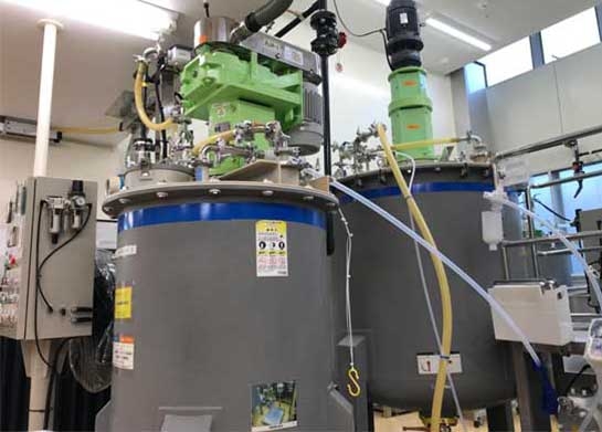
Who makes the CMP slurry that powers the world’s most advanced semiconductor fabs — and how do you evaluate them for your specific process and supply chain needs? This guide ...
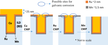
As semiconductor technology crosses into the angstrom era, CMP slurry formulation science faces its most demanding challenges yet. Mechanically fragile ultra-low-k dielectrics, new metal conductors with no CMP precedent, three-dimensional ...
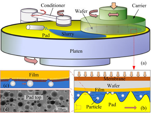
CMP slurry and CMP pad are the two primary consumables in every chemical-mechanical planarization process — and they are so deeply interdependent that optimizing one without accounting for the other ...
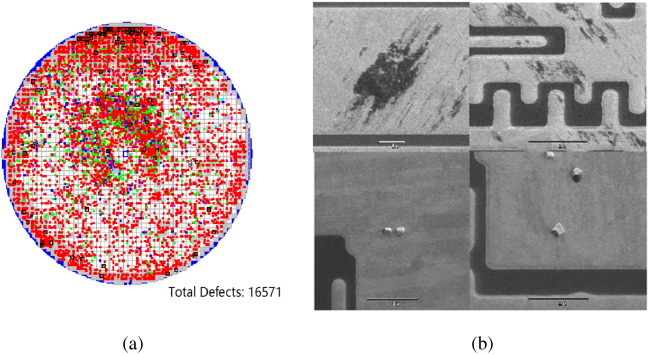
In semiconductor manufacturing, a CMP defect is not merely a surface imperfection — it is a direct threat to device yield, reliability, and the tens of thousands of process steps ...
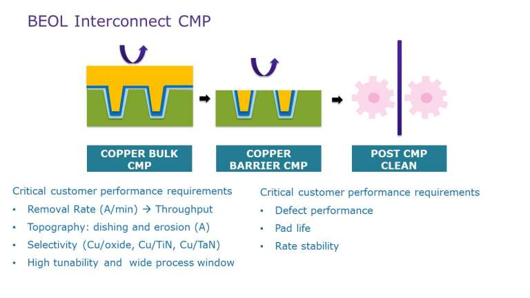
Copper CMP Slurry: Dual Damascene Process, Formulation & Defect Control — Complete Engineering Guide
Copper CMP is the most chemically complex and process-sensitive step in BEOL semiconductor manufacturing. A three-stage polishing sequence — each requiring a fundamentally different slurry chemistry — must deliver bulk ...
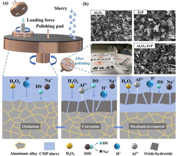
What actually goes into a CMP slurry — and why does every ingredient matter? This is the definitive technical guide to CMP slurry composition: abrasive particle science, chemical additive functions, ...
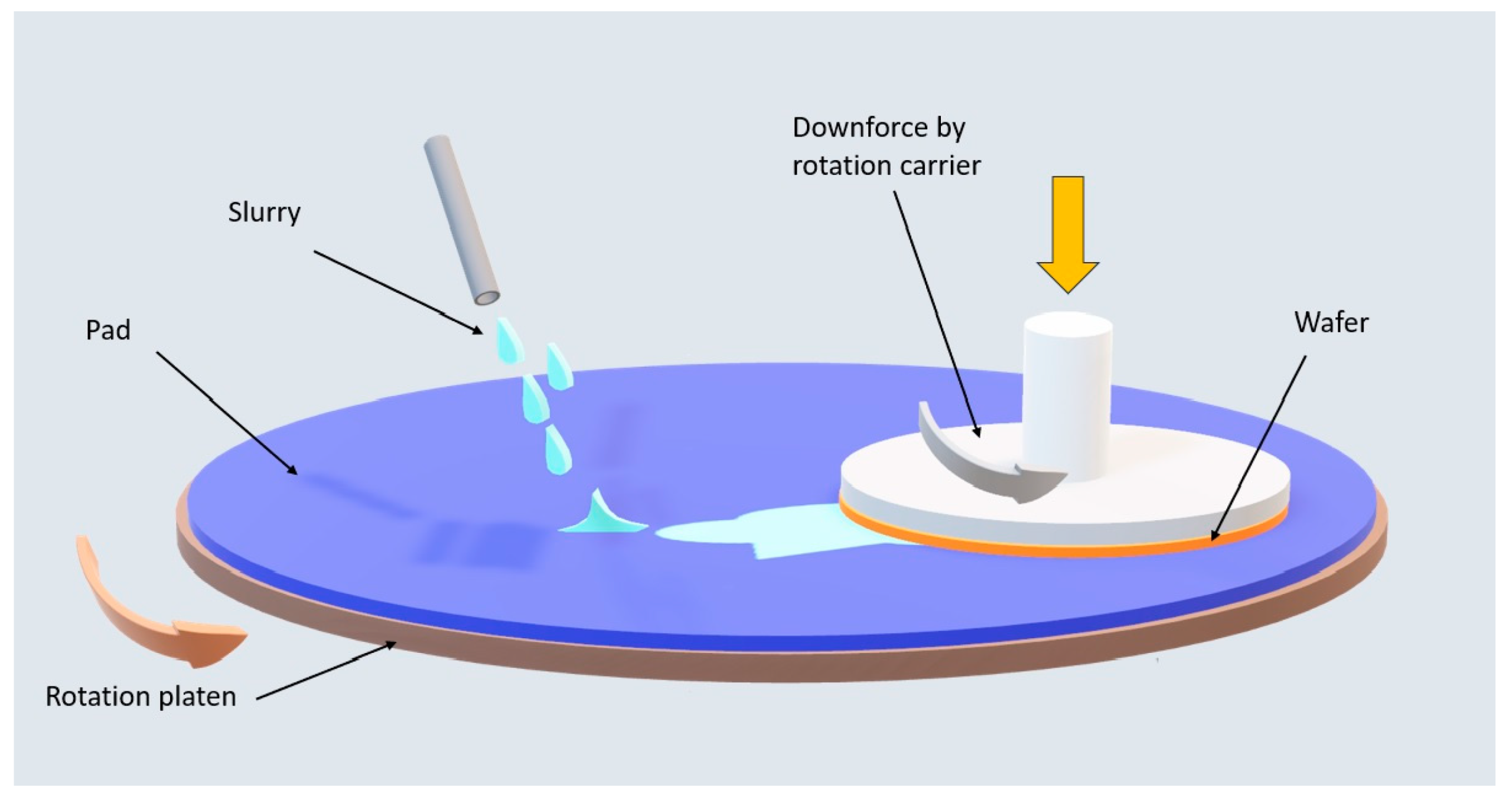
From wafer-level planarization at the 3nm node to advanced packaging for chiplets, CMP slurry is the consumable that makes modern semiconductor manufacturing possible. This guide covers everything you need to ...
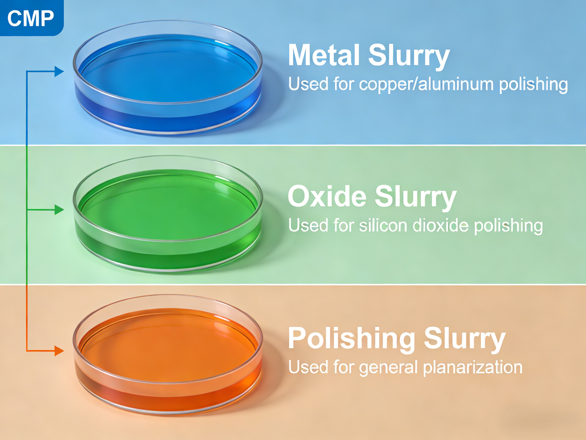
Not all CMP slurries are created equal. Each semiconductor polishing step demands a uniquely formulated slurry — different abrasive chemistry, different pH, different selectivity profile. This guide breaks down every ...
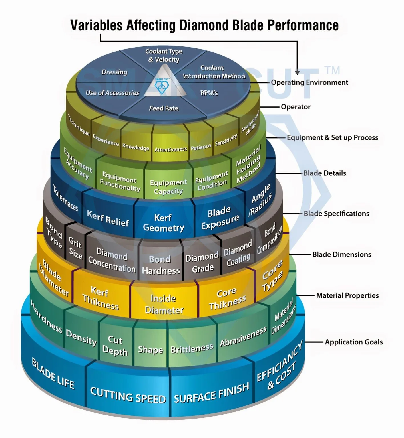
Choosing the right dicing blade is one of the most critical engineering decisions in semiconductor wafer singulation. Unlike many consumables, a dicing blade directly determines kerf loss, die edge quality, ...
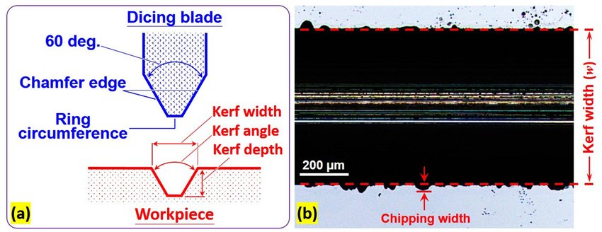
Ширина пильного полотна - критический параметр, напрямую определяющий контроль пропила, точность резки и стабильность траектории движения пильного полотна при обработке пластин. Хотя ширина полотна часто обсуждается вместе с ...
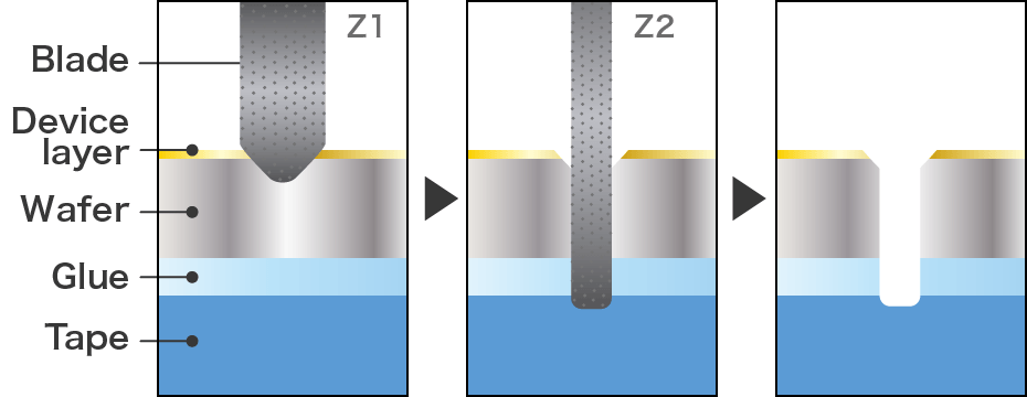
Толщина пильного диска - один из наиболее важных, но часто недопонимаемых параметров при обработке пластин. Толщина лезвия напрямую определяет потери пропила, влияет на механическую прочность матрицы и должна оставаться ...
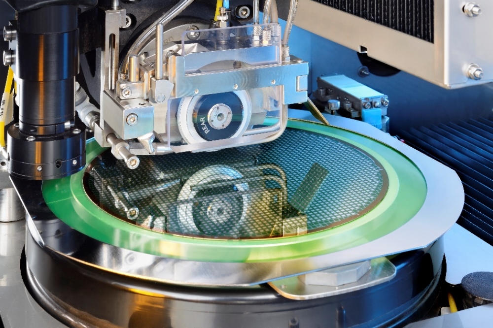
При обработке полупроводниковых пластин производительность алмазных лезвий неотделима от характеристик оборудования для обработки пластин. Даже хорошо спроектированное лезвие не сможет обеспечить стабильные результаты резки ...


