
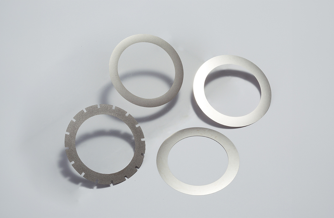
用于晶片切割的金刚石切割片
Diamond dicing blades are the core cutting tools used in modern semiconductor wafer singulation. From a product engineering perspective, a diamond dicing blade is not a generic consumable but a ...
Diamond dicing blades are the core cutting tools used in modern semiconductor wafer singulation. From a product engineering perspective, a diamond dicing blade is not a generic consumable but a ...
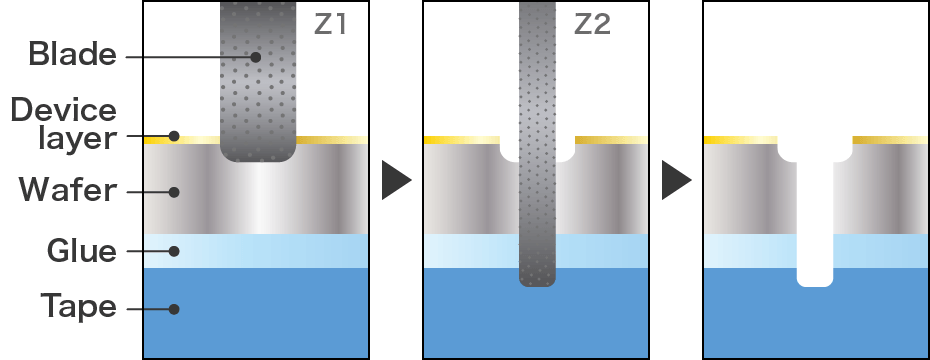
The blade dicing process is the most widely adopted wafer singulation method in semiconductor manufacturing. Despite the emergence of alternative technologies such as laser dicing and stealth dicing, blade dicing ...
Dicing blade technology forms the technical foundation of wafer singulation in semiconductor manufacturing. While the dicing process itself appears mechanically simple, the cutting behavior at the blade–wafer interface is governed ...
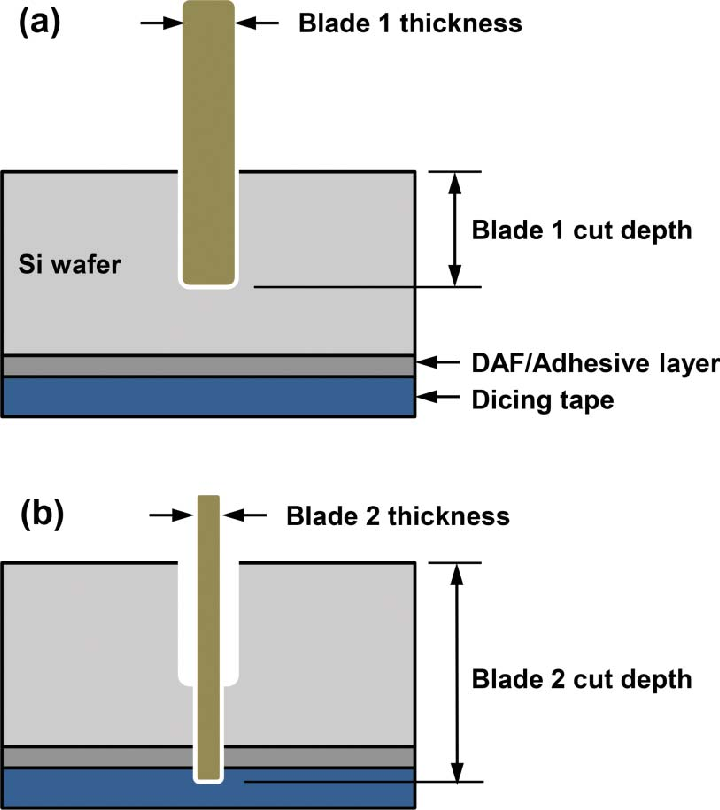
晶圆切割刀片是半导体制造中使用的精密切割工具,用于将加工好的晶圆分离成单个晶粒。虽然切割是晶圆制造的最后步骤之一,但其 ...
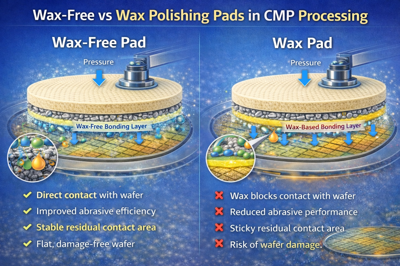
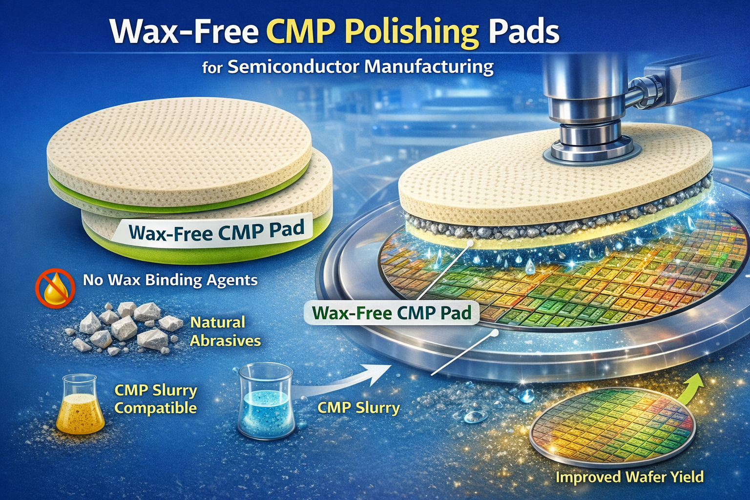
在 CMP 中,抛光垫材料决定了基本的机械、化学和摩擦学相互作用,最终决定了平面化效率、缺陷率和工艺稳定性。对于无蜡 CMP 研磨垫而言,材料的选择成为...
在现代半导体制造中,CMP 不再是一个孤立的单元操作,而是与上游沉积、下游清洗和整体产量管理相互作用的紧密集成工艺模块。采用 ...
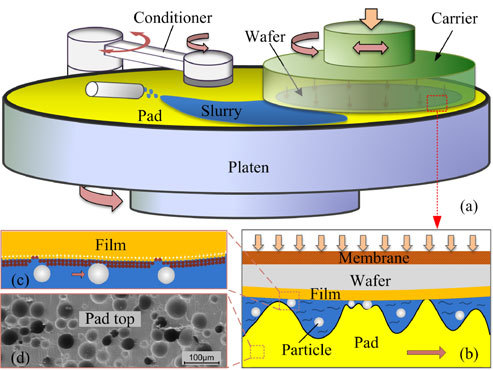
在化学机械平坦化(CMP)过程中,抛光垫不仅仅是一个消耗品表面,还是一个关键的工艺组件,直接影响到晶片的平坦度、材料去除率(MRR)、缺陷率、成品率 ...
目录 1. 引言:无蜡垫工作原理为何重要 2.CMP 系统背景:作为机械子系统的无蜡焊盘 3.无蜡焊盘-晶片接触力学 ...
目录 1.技术概述:吸附取代蜡粘合 2.无蜡垫吸附力的基本来源 3.吸附垫微结构设计与吸附效率 ...
目录 1.无蜡 CMP 抛光垫片的定义和技术范围 2.无蜡抛光垫的产品形式和设计意图 3.核心技术:无蜡吸附基本原理 ...
高精度表面加工材料
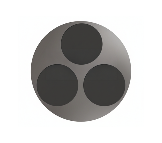
抛光泥浆 - 研磨垫 - 半导体切割刀片
关键生产步骤的可靠性和一致性。.
Copyright ©2026 无锡市吉智电子科技有限公司 All Rights Reserved.
电话
+(86) 180-6835-1533
电子邮件
contact@jeez-semicon.com
地址
中国江苏无锡


