
CMP 研磨垫材料和结构说明
在 CMP 中,抛光垫材料决定了基本的机械、化学和摩擦学相互作用,最终决定了平面化效率、缺陷率和工艺稳定性。对于无蜡 CMP 研磨垫而言,材料的选择变得更加重要,因为晶片固定、力传递和研磨液相互作用直接受研磨垫的体积和表面特性而非辅助蜡层的影响。本文件对 CMP 研磨垫材料进行了材料机制层面的分析,重点关注聚合物体系、微结构设计、机械参数、磨损行为及其对无蜡研磨垫结构的具体影响。目录 CMP 研磨垫材料概述 聚合物化学和基质设计 微结构和 ...
在 CMP 中,抛光垫材料决定了基本的机械、化学和摩擦学相互作用,最终决定了平面化效率、缺陷率和工艺稳定性。对于无蜡 CMP 研磨垫而言,材料的选择变得更加重要,因为晶片固定、力传递和研磨液相互作用直接受研磨垫的体积和表面特性而非辅助蜡层的影响。本文件对 CMP 研磨垫材料进行了材料机制层面的分析,重点关注聚合物体系、微结构设计、机械参数、磨损行为及其对无蜡研磨垫结构的具体影响。目录 CMP 研磨垫材料概述 聚合物化学和基质设计 微结构和 ...
在现代半导体制造中,CMP 不再是一个孤立的单元操作,而是与上游沉积、下游清洁和整体产量管理相互作用的紧密集成工艺模块。无蜡 CMP 抛光垫的采用从根本上改变了晶圆的固定、装载、抛光和释放方式,这就要求刻意进行工艺整合,而不是简单地更换耗材。本文重点介绍如何将无蜡抛光垫实际集成到 CMP 工艺中,哪些工艺参数会受到直接影响,以及晶圆厂如何利用无蜡架构来提高工艺稳定性、良率一致性和成本效益。目录 在 CMP 流程中集成无蜡抛光垫...
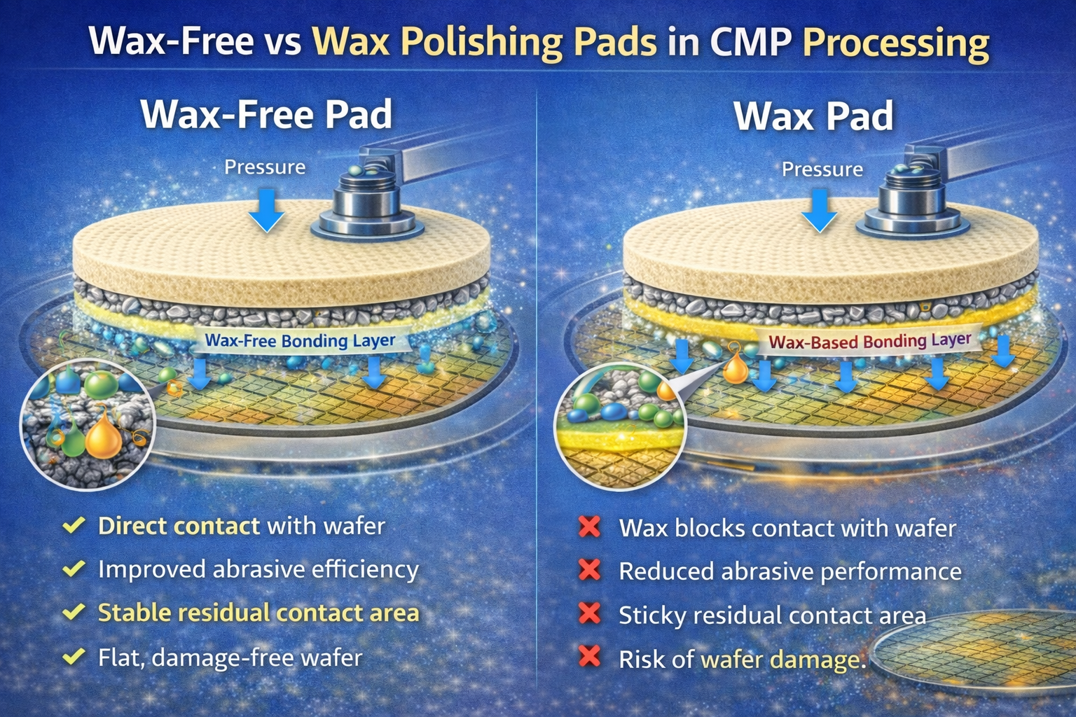
In chemical mechanical planarization (CMP), the polishing pad is not merely a consumable surface but a critical process component that directly affects wafer flatness, material removal rate (MRR), defectivity, yield stability, and overall cost of ownership (CoO). Among available pad architectures, wax-free CMP polishing pads and traditional wax-based polishing pads represent two fundamentally different philosophies of wafer fixation, force transmission, and contamination control. This page provides an engineering-level comparison between wax-free and wax polishing pads, focusing on structural design, adsorption mechanisms, process behavior, defect risks, maintenance complexity, and long-term manufacturing economics. The goal is to support data-driven decision-making rather than ...
Table of Contents 1. Introduction: Why Wax-Free Pad Working Principles Matter 2. CMP System Context: Wax-Free Pads as a Mechanical Subsystem 3. Pad–Wafer Contact Mechanics Without Wax Bonding 4. Wafer Loading and Initial Adsorption Formation 5. Pressure Ramp-Up and Adsorption Force Stabilization 6. Slurry Introduction and Frontside–Backside Decoupling 7. Steady-State CMP: Dynamic Adsorption Under Motion 8. Thermal and Mechanical Stability During CMP Operation 9. Controlled Wafer Release and De-Adsorption Behavior 10. Manufacturing-Level Process Control Implications 1. Introduction: Why Wax-Free Pad Working Principles Matter Understanding how wax-free polishing pads work is essential for modern CMP process development because wafer ...
Table of Contents 1. Technology Overview: Adsorption as a Replacement for Wax Bonding 2. Fundamental Sources of Adsorption Force in Wax-Free Pads 3. Pad Microstructure Design and Adsorption Efficiency 4. Contact Mechanics at the Pad–Wafer Interface 5. Tunable Engineering Parameters Affecting Adsorption 6. Adsorption Stability Under CMP Operating Conditions 7. Adsorption Degradation and Failure Modes 8. Position of Adsorption Technology Within CMP Systems 1. Technology Overview: Adsorption as a Replacement for Wax Bonding Wax-free adsorption polishing pad technology was developed to eliminate the inherent limitations of wax-based wafer bonding in CMP. Traditional wax layers introduce viscoelastic behavior, thermal sensitivity, ...
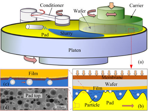
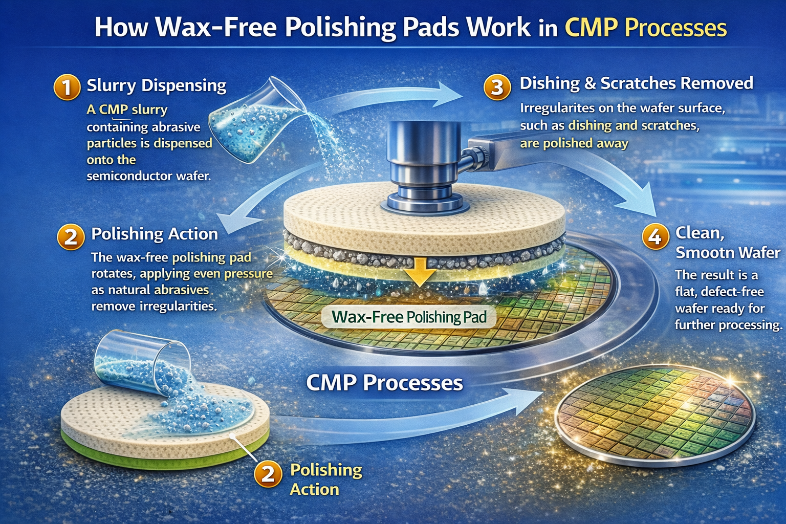
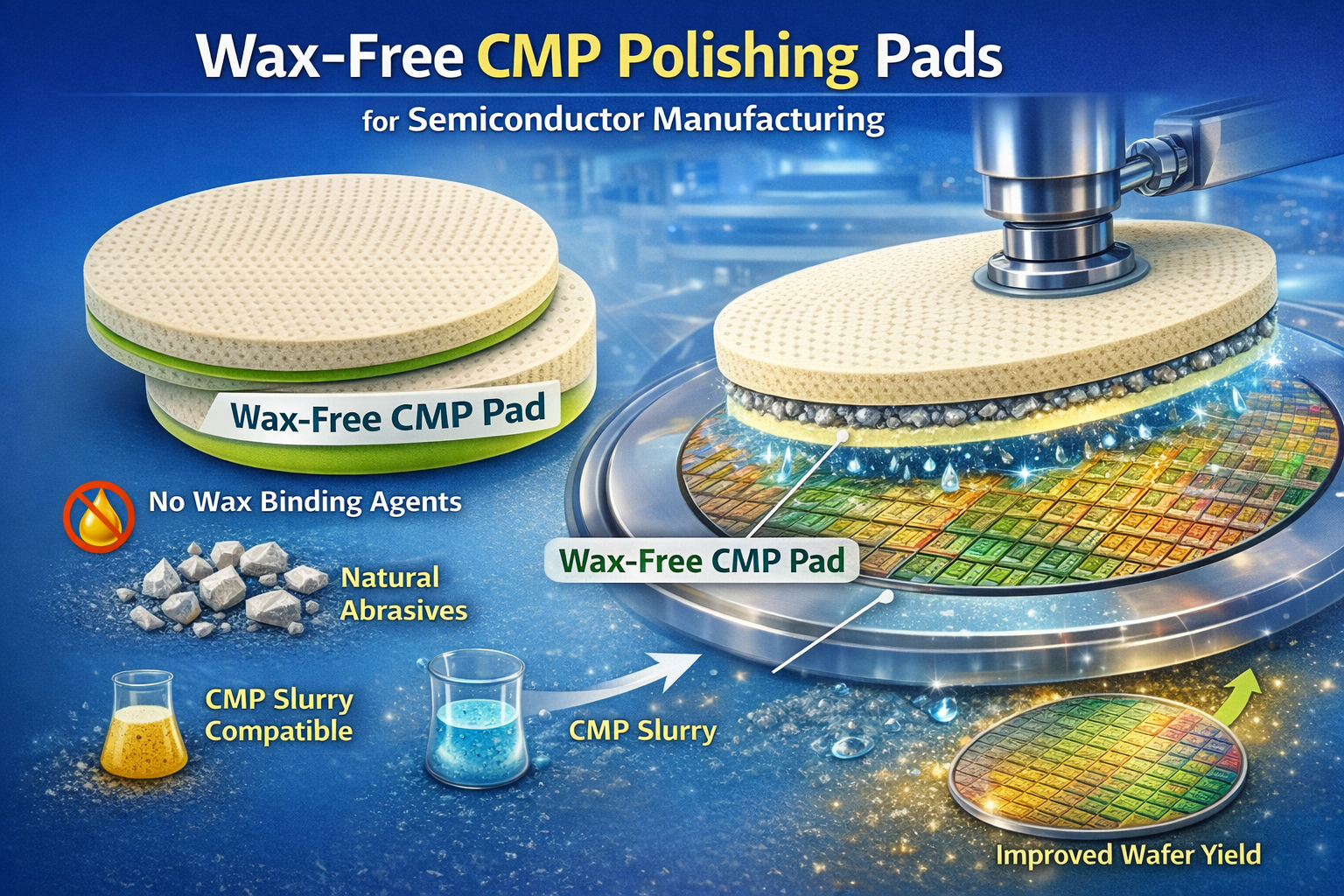
Table of Contents 1. Definition and Technical Scope of Wax-Free CMP Polishing Pads 2. Product Forms and Design Intent of Wax-Free Polishing Pads 3. Core Technology: Wax-Free Adsorption Fundamentals 4. How Wax-Free CMP Polishing Pads Work in Practice 5. Wax-Free vs Wax-Based CMP Polishing Pads 6. Integration of Wax-Free Pads in CMP Processes 7. Material and Structural Foundations of Wax-Free CMP Pads 1. Definition and Technical Scope of Wax-Free CMP Polishing Pads Wax-free CMP polishing pads are engineered wafer holding and polishing interfaces designed to operate without wax or adhesive bonding layers during chemical mechanical planarization. Unlike traditional wax-based ...
An Engineering-Level Decision Framework for Semiconductor Wafer Polishing Table of Contents 1. Introduction 2. First-Principles Approach to Slurry Selection 3. Wafer Material Considerations 4. Matching Slurry Type to CMP Process 5. Key Performance Metrics 6. Process Window & Margin Engineering 7. Compatibility with CMP Polishing Pads 8. Defectivity & Yield Risk Assessment 9. CMP Tool & Delivery System Constraints 10. High-Volume Manufacturing (HVM) Considerations 11. Common CMP Slurry Selection Mistakes 12. Qualification & Ramp-Up Strategy 13. Engineering Summary 1. Introduction Choosing the right CMP slurry is one of the most consequential decisions in semiconductor manufacturing. Unlike many consumables, slurry ...
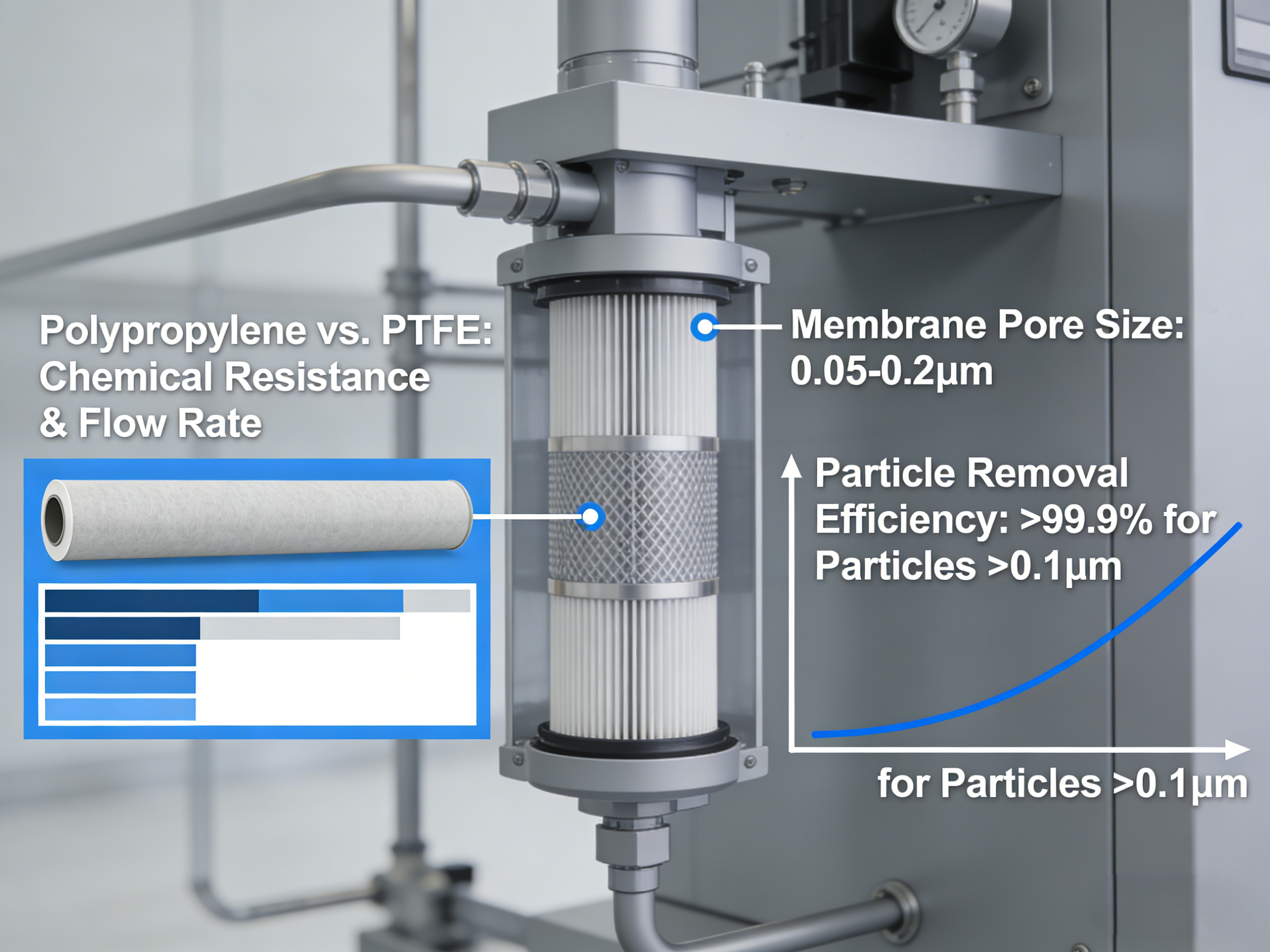
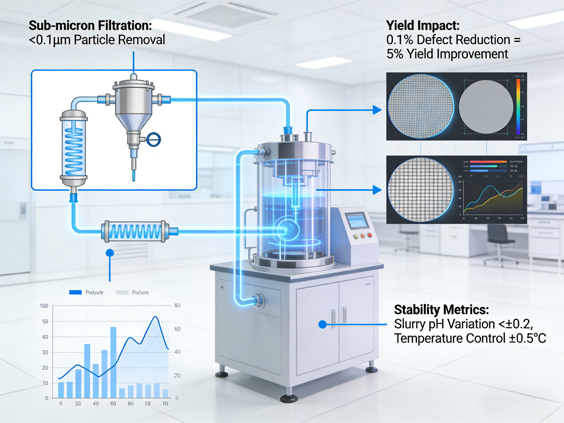
Filter Media, Housing Design, and Point-of-Use Control in Semiconductor CMP Table of Contents 1. Overview of CMP Slurry Filters 2. Role of Filters in CMP Yield Control 3. Filter Media Materials 4. Absolute vs Nominal Rating 5. Pore Size Distribution & Cutoff Behavior 6. Filter Housing Design 7. Point-of-Use (POU) Filtration 8. Chemical Compatibility & Extractables 9. Performance Data & Lifetime Modeling 10. Failure Modes & Root Cause Analysis 11. HVM Filter Management Strategy 12. How to Select CMP Slurry Filters 13. Future Trends 1. Overview of CMP Slurry Filters CMP slurry filters are precision components designed to remove ...
Particle Control, Yield Protection, and Process Stability in Semiconductor CMP Table of Contents 1. Introduction 2. Why Filtration Is Critical in CMP 3. Particle Sources in CMP Slurry Systems 4. Particle Size vs Defect Mechanisms 5. CMP Slurry Filter Technologies 6. Filter Pore Size Selection Strategy 7. Chemical Compatibility & Slurry Stability 8. Experimental Data & Filtration Performance 9. Filtration Process Window 10. Integration with CMP Tools 11. Filtration Failure Modes & RCA 12. HVM Filtration Strategy 13. Future Trends 1. Introduction CMP slurry filtration is one of the most underestimated yet yield-critical elements in semiconductor manufacturing. While slurry ...
Table of Contents 1. Introduction to Tungsten CMP 2. Tungsten CMP Applications in Semiconductor Devices 3. Material Properties of Tungsten Relevant to CMP 4. Chemical–Mechanical Removal Mechanism 5. Tungsten CMP Slurry Composition Architecture 6. Chemical Kinetics & Rate-Limiting Steps 7. Engineering Parameters & Experimental Data 8. Process Window & Control Maps 9. Defect Mechanisms & Root Cause Analysis 10. High-Volume Manufacturing Challenges 11. Slurry Selection & Optimization Guidelines 12. Future Trends in Tungsten CMP Slurry 1. Introduction to Tungsten CMP Tungsten Chemical Mechanical Planarization (CMP) plays a critical role in semiconductor manufacturing, particularly for contact plug and via fill ...
高精度表面加工材料
抛光泥浆 - 研磨垫 - 半导体切割刀片
关键生产步骤的可靠性和一致性。.
Copyright ©2026 无锡市吉智电子科技有限公司 All Rights Reserved.
电话
+(86) 180-6835-1533
电子邮件
contact@jeez-semicon.com
地址
中国江苏无锡


