CMP Semiconductor:The Complete Guide to Chemical Mechanical Planarization
Everything engineers, procurement specialists, and researchers need to know about Chemical Mechanical Planarization — from first principles to advanced-node challenges, consumable selection, defect control, and the future of CMP in 3D IC fabrication.
- What Is CMP?
- Why CMP Matters in Chip Fabrication
- How the CMP Process Works Step by Step
- Key CMP Consumables: Slurry & Polishing Pad
- Types of CMP: Oxide, Copper & Tungsten
- CMP Defects & Yield Control
- CMP in Advanced Nodes & 3D IC
- Post-CMP Cleaning
- CMP Equipment & Market Overview
- Why Choose JEEZ for CMP Consumables
- 常见问题
What Is CMP in Semiconductor Manufacturing?
化学机械平坦化 (CMP) — also called Chemical Mechanical Polishing — is a critical wafer-surface-finishing process used throughout integrated circuit (IC) fabrication. It combines controlled chemical reactions with mechanical abrasion to remove excess material from a wafer’s surface and achieve the exceptional flatness required for each successive layer of a microchip.
The term “planarization” precisely describes the objective: to create a globally planar — that is, perfectly flat — surface so that photolithography systems can project circuit patterns with nanometer-level accuracy. Without CMP, the cumulative topography built up by successive deposition and etching steps would quickly exceed the depth-of-field tolerance of modern lithography optics, making reliable patterning impossible.
First disclosed by IBM in the late 1980s and commercially demonstrated by Intel on its Pentium processor in 1993, CMP has since become one of the most-used process steps in any modern fab. A leading-edge chip today may undergo 20 or more distinct CMP steps — polishing oxide inter-layer dielectrics (ILD), copper interconnects, tungsten plugs, barrier metals, and shallow trench isolation (STI) fills, among others.
Chemical Component
Reactive agents in the slurry soften or oxidise the surface material, enabling low-force removal and high selectivity between layers.
Mechanical Component
Abrasive particles in the slurry, combined with pad pressure and relative motion, physically remove the chemically modified material.
Planarization Outcome
The synergy of chemical and mechanical action produces a globally flat surface within Angstrom-level tolerance — impossible with either mechanism alone.
Why CMP Matters in Chip Fabrication
Modern integrated circuits are three-dimensional structures built layer by layer on a silicon wafer. Each deposition step adds material; each etching step removes it. Without periodic flattening, the cumulative surface topography becomes unmanageable. CMP is the solution that keeps the manufacturing process on track at every critical stage.
Enabling Multi-Level Metallization
Today’s processors and memory chips require 10 to 18 or more metal interconnect layers. Each layer must be deposited on a flat surface so that via holes can be etched with uniform depth and metal fills are void-free. CMP of the inter-layer dielectric after each metal layer makes this stacking possible, directly enabling Moore’s Law scaling.
Photolithography Depth-of-Field Control
Extreme ultraviolet (EUV) lithography systems used at 7 nm and below have a depth-of-field measured in tens of nanometers. Any surface height variation across the wafer that exceeds this tolerance causes out-of-focus patterning and fatal defects. CMP routinely delivers surface non-uniformity (WIWNU) below 1 nm across 300 mm wafers, keeping the wafer reliably within the lithography focus budget.
Shallow Trench Isolation (STI)
STI is the technique that electrically isolates adjacent transistors. After oxide deposition into etched trenches, CMP removes excess oxide from the field regions, leaving a planarized surface flush with the silicon nitride stop layer. This process defines the precise geometry of every transistor on the chip and is one of the earliest CMP applications in front-end-of-line (FEOL) processing.
Copper Dual-Damascene Interconnects
Since Intel’s landmark copper introduction in 1998, the entire interconnect stack of high-performance chips has been built using the dual-damascene process, which relies entirely on CMP to remove overburden copper and barrier metal after electrochemical deposition (ECD). Without reliable copper CMP, modern multi-GHz processors, AI accelerators, and memory chips simply could not be manufactured.
Industry impact in 2026
The global CMP consumables market — comprising polishing slurries, polishing pads, pad conditioners, and cleaning solutions — exceeded USD 6.8 billion in 2025 and continues to grow, driven by capacity expansions at TSMC, Samsung, Intel Foundry, and SK Hynix. CMP consumables represent one of the highest-recurring cost lines in any wafer fab’s operating budget.
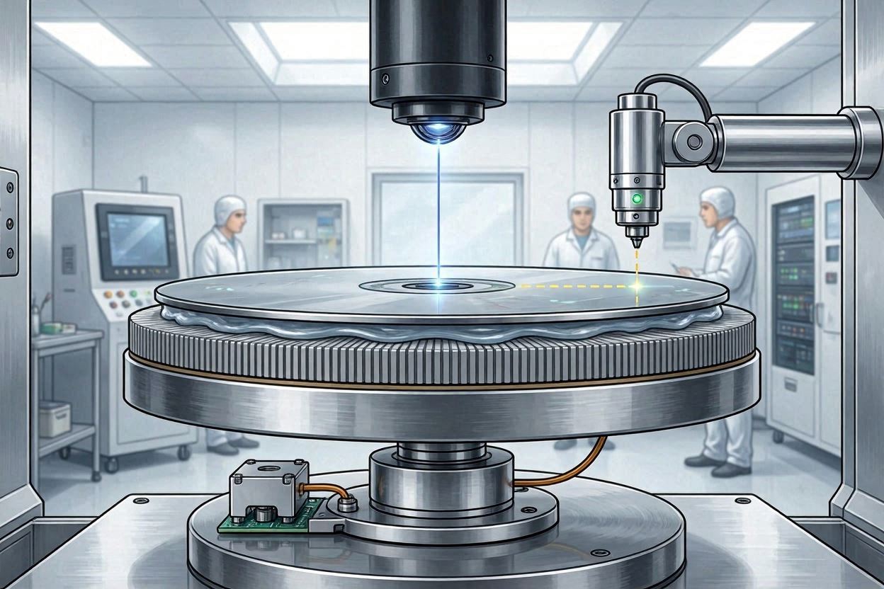
How the CMP Process Works Step by Step
Understanding the mechanics of CMP is essential for optimising removal rate, uniformity, and defectivity. The process involves five tightly integrated stages. For a detailed engineering breakdown of each stage, refer to our dedicated guide: CMP Process Step-by-Step: How Wafer Polishing Works.
-
1
Substrate Preparation & Loading
The silicon wafer is mounted face-down in a rotating carrier head. A compliant backing film distributes load uniformly across the wafer’s backside. Precise carrier head pressure — typically 1 to 6 psi depending on film type — is set before polishing begins. The wafer is held by vacuum during transfer to prevent surface contamination.
-
2
Slurry Delivery
CMP slurry — a colloidal suspension of abrasive nanoparticles (typically silica SiO₂ or ceria CeO₂, 50–250 nm diameter) in an aqueous chemical solution — is dispensed onto the rotating polishing pad at a controlled flow rate of 100–300 mL/min. The chemical formulation is tuned for the specific film being polished: oxidising agents for copper, alkaline pH for oxide, acidic pH for tungsten.
-
3
Mechanical Polishing
The carrier head rotates (typically 30–120 RPM) while the platen — a large flat disk covered with the polishing pad — rotates independently. The relative velocity between the wafer and pad, combined with the applied downforce, drives abrasive particles across the wafer surface. The chemical component simultaneously reacts with and softens the surface film, enabling material removal at rates of 100–1,500 Å/min depending on film type and process conditions.
-
4
Endpoint Detection
Reaching the precise target thickness — often within ±5 nm across 300 mm — requires real-time endpoint detection. Modern CMP tools use optical interferometry (reflectometry) or motor current sensing to detect the moment the polishing front reaches the underlying stop layer. Multi-zone pressure control in the carrier head then allows zone-by-zone thickness correction to achieve within-wafer non-uniformity (WIWNU) below 1%.
-
5
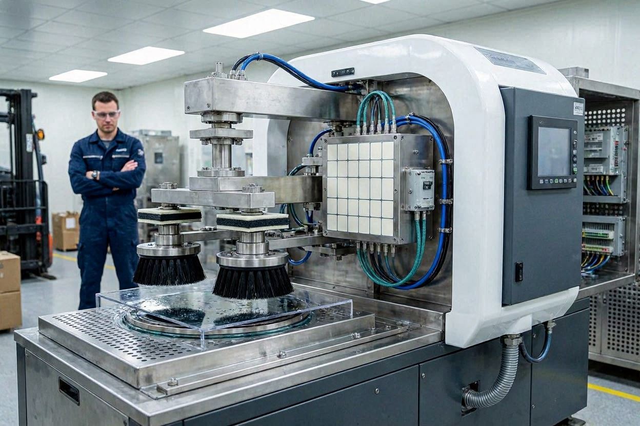
Post-CMP Cleaning
Immediately after polishing, the wafer is transferred — still wet — to an integrated brush-scrub cleaning module. Polyvinyl alcohol (PVA) brushes in combination with carefully formulated cleaning chemistry remove residual slurry particles, polishing by-products, and metallic contaminants. Megasonic-assisted cleaning may be added for sub-7 nm applications. The wafer is then rinsed with ultra-pure water and spin-dried before the next process step.
Key CMP Consumables: Slurry & Polishing Pad
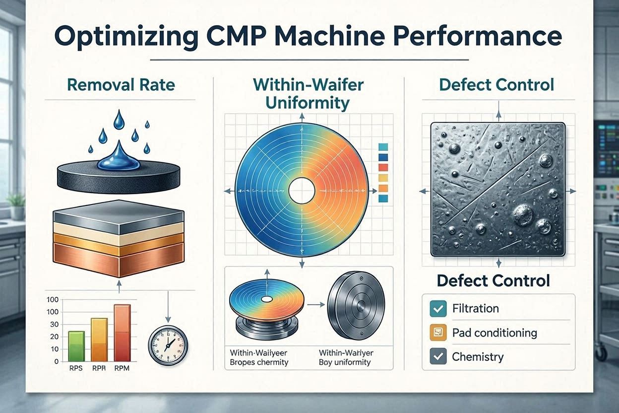
The performance of any CMP process is governed by two primary consumables: the polishing slurry and the polishing pad. Together, they define removal rate, selectivity, surface quality, and defect density. Selecting the right combination — and maintaining consistent quality — is one of the most consequential decisions a process engineer makes.
CMP Polishing Slurry
A CMP slurry is an engineered colloidal dispersion containing three functional components: abrasive particles, chemical agents, and performance-modifying additives. The abrasive provides the mechanical cutting action; the chemicals control reaction selectivity; the additives — surfactants, chelating agents, corrosion inhibitors, polymers — fine-tune particle stability, surface interactions, and post-polish cleanliness.
Abrasive selection is the first critical decision. Silica (SiO₂) slurries are the workhorse for oxide and STI CMP, offering tunable selectivity and low defectivity. Ceria (CeO₂) slurries achieve dramatically higher oxide removal rates — up to 10× that of silica — and superior planarization efficiency, making them preferred for STI and pre-metal dielectric applications. Alumina (Al₂O₃) is used for tungsten CMP. The particle size distribution (PSD), particularly the concentration of large aggregates above 1 µm (so-called “large particles” or LPCs), directly controls scratch defect density.
泥浆 pH 值 determines both removal rate and surface chemistry. Oxide slurries operate at pH 10–11 to keep silica particles negatively charged and well-dispersed. Copper slurries are typically acidic (pH 2–4) with oxidisers such as hydrogen peroxide (H₂O₂) to form a soft copper oxide layer that is then abraded away. Tungsten slurries use a similar oxidative mechanism at near-neutral pH.
For a comprehensive guide to slurry types, formulation strategies, and selection criteria by application, see our dedicated article: CMP Slurry Guide: Types, Selection & Optimization.
CMP Polishing Pad
The polishing pad is the physical interface between the slurry and the wafer. Its mechanical properties — hardness, compressibility, surface texture, and groove geometry — control how slurry is transported to the wafer surface, how uniformly pressure is distributed, and ultimately how well the wafer is planarized.
Conventional CMP pads are made from polyurethane foam, with a porous microstructure that retains slurry and renews itself as material is abraded away. The pad surface texture degrades with use — a process called “glazing” — which causes removal rate to drift. To counteract glazing, a diamond pad conditioner is used periodically to restore pad surface roughness (Ra) to specification. Pad conditioning is itself a critical process variable that significantly impacts pad lifetime, removal rate stability, and wafer-to-wafer repeatability.
Pad hardness represents a fundamental trade-off: harder pads (such as IC1000) deliver better global planarization efficiency but can increase micro-scratch defects. Softer, more compliant pads conform to local topography, reducing defects but sacrificing planarization efficiency. Many advanced CMP processes use a two-platen approach: a hard pad for primary removal followed by a soft buff pad for surface finish improvement.
For an in-depth breakdown of pad types, conditioning strategies, and advanced pad technologies such as fixed-abrasive and microreplication designs, visit our article: CMP Polishing Pad: Types, Selection & Performance Guide.
CMP Polishing Slurry
JEEZ manufactures and supplies a complete range of CMP slurries — oxide, STI, copper, tungsten, and barrier — engineered for 300 mm production environments. Our slurries are characterised by tight PSD control, batch-to-batch consistency, and low large-particle counts.
View Slurry Products →CMP Polishing Pads
JEEZ polishing pads are available in hard, soft, and multi-layer stack configurations, covering a broad range of CMP applications from oxide ILD to copper dual-damascene and advanced packaging. Custom groove patterns and pad dimensions are available on request.
View Pad Products →Types of CMP: Oxide, Copper & Tungsten
CMP is not a single monolithic process. Each material polished in a semiconductor fab demands a uniquely engineered chemistry, abrasive system, and process window. The three most prevalent types are oxide CMP, copper CMP, and tungsten CMP. Understanding their distinctions is essential for process integration and consumable qualification. For a side-by-side technical comparison, see: Copper CMP vs Tungsten CMP vs Oxide CMP: Full Comparison.
| CMP 类型 | 主要应用 | 磨料 | Chemistry | 主要挑战 |
|---|---|---|---|---|
| Oxide / STI CMP | ILD planarization, STI fill | Silica or Ceria | Alkaline (pH 10–11) | High oxide-to-nitride selectivity; dishing in wide trenches |
| 铜 CMP | Dual-damascene interconnects | Silica + oxidiser | Acidic (pH 2–4), H₂O₂ | Erosion, dishing, corrosion; barrier removal selectivity |
| Tungsten CMP | Contact and via plugs | 氧化铝 | Near-neutral, Fe³⁺ or H₂O₂ | High removal rate while protecting thin oxide stop layer |
| Barrier Metal CMP | TaN/Ta barrier removal | Colloidal silica | Slightly acidic + corrosion inhibitor | Selectivity between barrier, copper, and low-k dielectric |
| Low-k Dielectric CMP | Back-end porous dielectrics | Fine colloidal silica | Near-neutral; gentle formulation | Mechanical fragility of porous low-k films; delamination risk |
Oxide & STI CMP
Oxide CMP was the original CMP application — invented to planarize inter-level dielectric (ILD) silicon dioxide between aluminum interconnect layers. Today its most demanding form is STI CMP, in which silicon dioxide deposited into shallow trenches must be polished back precisely to a silicon nitride stop layer. Ceria-based slurries are preferred here because of their inherently high oxide-to-nitride selectivity (often exceeding 100:1), which provides a natural endpoint mechanism and minimises nitride erosion. Over-polishing in STI can cause “dishing” — a concave recess in the oxide fill — which degrades transistor isolation and increases leakage current.
铜 CMP
Copper CMP is arguably the most chemically complex CMP type. It typically involves a three-step sequence: bulk copper removal, barrier metal removal, and a buff/clean step. The slurry must simultaneously oxidise copper (via H₂O₂ or similar oxidiser), chelate the copper oxide for dissolution, and apply corrosion inhibitors (most commonly benzotriazole, BTA) to suppress over-etching in recessed regions. The competing demands for high removal rate in raised areas and corrosion protection in recessed areas create a narrow process window that tightens with every technology node.
Tungsten CMP
Tungsten CMP removes excess tungsten deposited by CVD to fill contact holes and vias. Because tungsten is very hard, alumina abrasives are typically used to achieve practical removal rates of 1,000–2,000 Å/min. The primary integration challenge is stopping precisely at the thin underlying oxide layer without removing excessive amounts of it — a selectivity requirement that demands careful optimisation of oxidiser concentration and abrasive loading. Residual tungsten “stringers” at the field level are a critical yield detractor that slurry formulation and process time control must eliminate.
CMP Defects & Yield Control
Defectivity management is the single greatest challenge in CMP process engineering. Even a well-optimised process that achieves excellent removal rate and uniformity can deliver poor yield if defect density is not tightly controlled. The principal CMP defect categories, their root causes, and mitigation strategies are explored in detail in our guide: CMP Defect Types, Root Causes & Yield Improvement.
Scratch Defects
Micro-scratches are caused by large abrasive particles or hard agglomerates in the slurry impacting the wafer surface under load. They represent the most critical CMP defect class because they can sever metal lines, cause gate dielectric damage, and introduce stress concentrations that accelerate reliability failures. Controlling slurry large-particle count (LPC) — the number of particles above 0.5 µm per mL — is the primary mitigation lever. Slurry filtration at point-of-use (POU), proper slurry storage temperature, and avoidance of freeze-thaw cycles are all essential handling practices.
挖泥和侵蚀
垂钓 refers to a concave topography at the centre of wide metal or oxide features after CMP. It arises because the polishing pad — being compliant — conforms slightly into wide, recessed structures, continuing to remove material after the surrounding field surface has reached the stop layer. 侵蚀 describes the thinning of the dielectric field around dense arrays of metal features, resulting from the locally high pattern density. Both phenomena increase with feature width and array density, and both worsen as technology nodes shrink. Pattern-density-aware slurry formulations and advanced endpoint systems are the primary controls.
Residues & Contamination
Residual slurry particles and polishing by-products that are not removed during post-CMP cleaning can cause electrical shorts, leakage paths, or serve as nucleation sites for subsequent process failures. Metallic contamination — particularly copper ions on silicon surfaces — is especially damaging, as copper diffuses readily through silicon dioxide and poisons transistor junctions. This is why post-CMP cleaning chemistry and process control are given equal engineering attention as the polish step itself. See our comprehensive post-CMP cleaning resource: Post-CMP Cleaning: Methods, Challenges & Best Practices.
脱层
As fabs transition to ultra-low-k (ULK) and extreme low-k (ELK) dielectrics at advanced nodes, the mechanical fragility of these porous films introduces the risk of delamination — film separation at an interface — under CMP polishing stress. Mitigation requires reducing downforce, using softer polishing pads, and reformulating slurries with lower abrasive loading and improved surfactant packages that reduce interfacial shear stress.
CMP in Advanced Nodes & 3D IC
As semiconductor technology advances beyond 3 nm and into the era of 3D stacked architectures, CMP faces challenges that fundamentally redefine what is required of both the process and the consumables. These challenges are explored comprehensively in our forward-looking analysis articles: CMP in Advanced Nodes: Challenges at 7nm, 5nm & Beyond 和 CMP in 3D IC & Heterogeneous Integration: New Frontiers.
Gate-All-Around (GAA) and CFET Requirements
At 3 nm and below, FinFET transistors give way to Gate-All-Around (GAA) nanosheet architectures and, looking ahead, complementary FET (CFET) structures. These require CMP steps with unprecedented uniformity — within-die non-uniformity targets below 0.3 nm — to selectively polish sacrificial silicon germanium (SiGe) layers from between silicon nanosheet channels. Achieving this demands ceria-based slurries with tuned SiGe-to-Si selectivity and real-time, multi-zone closed-loop thickness control.
New Materials: Cobalt, Ruthenium, and Low-Resistance Metals
Tungsten, which has dominated contact and local interconnect fill for decades, is being replaced at advanced nodes by cobalt (Co) and ruthenium (Ru) to reduce contact resistance. These new metals require entirely new slurry chemistries. Cobalt CMP is particularly challenging because cobalt is susceptible to corrosion and surface roughening in acidic environments, and cobalt ions are toxic at trace concentrations — driving stringent requirements for post-CMP cleaning and wastewater treatment.
3D NAND Flash: Hundreds of Layers
3D NAND flash memory — now reaching 300+ stacked layers in 2026 — relies on CMP to planarize thick oxide-nitride multilayer stacks and tungsten word-line fills repeatedly throughout fabrication. The sheer number of CMP steps and the extreme thickness of deposited films place unprecedented demands on consumable lifetime, removal rate stability, and within-wafer uniformity across a stack height exceeding 10 µm.
Advanced Packaging and Hybrid Bonding
Perhaps the most exciting frontier for CMP in 2026 is its role in advanced packaging, particularly hybrid bonding — a technique used to stack chiplets face-to-face with sub-micron pitch interconnects. Hybrid bonding requires CMP to produce copper pads and surrounding dielectric that are co-planar within 1–2 nm, with surface roughness below 0.3 nm Ra. This “nano-CMP” application demands novel slurry formulations, ultra-soft pads, and real-time in-situ metrology that far exceed the capabilities of conventional production CMP tools.
Post-CMP Cleaning
Post-CMP cleaning is not an afterthought — it is an integral part of the CMP module and arguably as technically demanding as the polishing step itself. After polishing, the wafer surface is covered with residual slurry abrasives, reaction by-products, dissolved metals, and organic contaminants. Removing these completely, without introducing new defects or damaging delicate surface structures, is the goal of the post-CMP clean.
For a full engineering treatment of cleaning chemistries, brush-scrub mechanics, megasonic technology, and advanced-node cleaning challenges, see: Post-CMP Cleaning: Methods, Challenges & Best Practices.
Brush Scrub Cleaning
The standard post-CMP cleaning method uses rotating polyvinyl alcohol (PVA) brushes that scrub both sides of the wafer simultaneously while cleaning chemistry is dispensed onto the surface. The brush provides a mechanical shear force that, combined with the chemical action of the cleaning solution, dislodges and removes particles. The chemistry is selected based on the surface material: acidic solutions with chelating agents for copper surfaces, dilute HF or HF/HCl mixtures for oxide surfaces, and alkaline solutions with surfactants for general particle removal.
The key variable in brush scrub performance is the electrostatic interaction between the particle, the wafer surface, and the brush. Controlling zeta potential through pH and surfactant selection — so that particles are repelled from both the wafer surface and the brush — is the underlying principle of effective particle removal. This is why even small changes in cleaning solution pH can dramatically affect particle removal efficiency (PRE).
Megasonic Cleaning
For sub-7 nm applications where tight feature geometries make brush scrubbing insufficient or potentially damaging, megasonic cleaning — in which acoustic energy at 800 kHz–1 MHz is applied to a liquid bath surrounding the wafer — offers a non-contact particle removal mechanism. The acoustic pressure waves create micro-streaming and cavitation near particle surfaces, dislodging them without direct mechanical contact. Megasonic cleaning is particularly effective for removing sub-100 nm particles that are difficult to dislodge by brush scrubbing alone.
Metallic Contamination Control
Copper contamination on silicon surfaces after copper CMP is an existential concern for FEOL device performance. Copper diffuses extremely rapidly through silicon dioxide and reaches the silicon/gate-oxide interface in milliseconds at elevated temperatures, causing threshold voltage shifts and increased junction leakage. Cleaning chemistries based on dilute HCl or chelating agents are used to complex and dissolve copper ions from the surface, typically achieving surface copper concentrations below 1×10¹⁰ atoms/cm² — the typical FEOL contamination budget.
CMP Equipment & Market Overview
The CMP equipment market is served by a small number of highly specialised tool vendors. Understanding the competitive landscape helps procurement teams evaluate both capital equipment and the consumables they use. For a detailed market analysis and buying guide, visit: CMP Equipment Market: Top Suppliers, Tools & Buying Guide.
Major CMP Tool Vendors
Applied Materials (AMAT) dominates the CMP tool market with its Reflexion and Mirra Mesa product families, which together account for an estimated 55–60% of global installed base. Ebara Corporation holds the second-largest share, particularly strong in Japan and Korea, with its FREX and EPO-222 platforms. DISCO Corporation and Revasum serve niche applications in silicon carbide (SiC) and compound semiconductor CMP. For advanced packaging and hybrid bonding applications, specialised bonding-preparation CMP tools from companies such as Tokyo Electron (TEL) and ACM Research are gaining traction in 2026.
Tool Architecture: Rotary vs. Linear
The dominant CMP tool architecture uses a circular rotating platen with a rotating carrier head — the design commercialised by Westech in the early 1990s. An alternative linear belt design offers theoretically more uniform slurry distribution and pad usage, but has not achieved widespread adoption in volume production. Multi-platen tools — with two or three polishing stations plus a dedicated cleaning station — are the production standard, enabling high wafer throughput (30–50 wafers per hour) while performing multiple sequential CMP steps in a single tool pass.
CMP Consumables Supply Chain
While equipment investment is a one-time capital expense, CMP consumables are a recurring operational cost that represents the largest ongoing expenditure in any CMP module. Polishing pads are replaced after 1,000–2,000 wafer passes; slurry is consumed at 100–300 mL per wafer polished. The consumables supply chain thus demands reliable vendors with globally consistent quality, robust logistics, and the technical application support to help fabs qualify new consumable lots without disrupting production.
Explore all CMP-related topics
Dive deeper into any specific aspect of CMP with our full cluster of technical articles, covering everything from slurry chemistry to 3D IC integration challenges.
Why Choose JEEZ for CMP Consumables
Jizhi Electronic Technology Co., Ltd. — operating under the brand JEEZ — is a dedicated manufacturer and global supplier of CMP consumables and precision semiconductor process materials. Founded on a philosophy of engineering-first product development, JEEZ brings together deep process chemistry expertise, rigorous quality management, and responsive technical support to deliver consumables that perform consistently in demanding production environments.
Our CMP Product Portfolio
CMP Polishing Slurry
Oxide, STI, copper, tungsten, barrier, and cobalt slurries engineered for production-grade removal rate stability, low LPC, and superior surface finish. Explore slurry products.
CMP Polishing Pads
Hard, soft, and multi-layer pad configurations for oxide ILD, copper, and advanced packaging applications, with custom groove patterns available. Explore pad products.
Dicing Blades
High-precision diamond dicing blades for wafer singulation across silicon, SiC, glass, and compound semiconductor substrates — engineered for minimum kerf width and chipping.
Global Supply & Technical Support
JEEZ operates a global supply network serving customers across North America, Europe, East Asia (Japan, Korea, Taiwan), Southeast Asia, and China. Our technical application team works directly with process engineers to support consumable qualification, lot-to-lot consistency verification, and process optimisation. We understand that in semiconductor manufacturing, supply chain reliability and technical responsiveness are not secondary concerns — they are requirements.
- Tight PSD control: all slurry batches characterised for D50, D90, and LPC using dynamic light scattering and single-particle optical sensing (SPOS).
- Lot-to-lot consistency: statistical process control (SPC) applied across all key formulation parameters, with certificate of analysis (CoA) supplied with each shipment.
- Application engineering: JEEZ engineers can assist with process qualification protocols, DOE design for CMP window optimisation, and in-fab troubleshooting.
- Regulatory compliance: products are formulated and documented to meet REACH, RoHS, and applicable regional chemical regulations for global deployment.
- Flexible packaging: available in drum, IBC, and small-volume sample quantities to support both R&D evaluation and high-volume production.
常见问题
Ready to Optimise Your CMP Process?
Talk to the JEEZ technical team about CMP slurry, polishing pads, or dicing blades. We work with fabs worldwide to qualify consumables and solve process challenges.
Contact JEEZ Technical Team →