
Kerf Width Variation in Wafer Dicing Root Causes and Control Methods
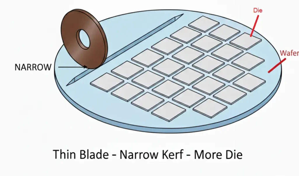
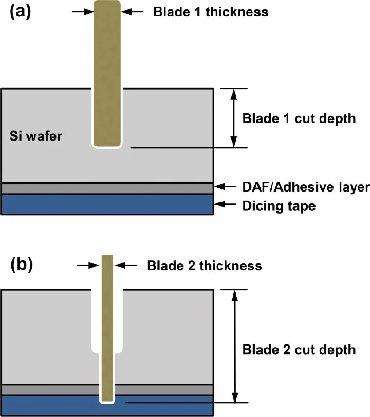
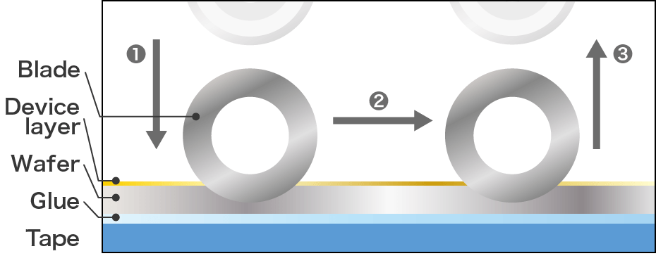
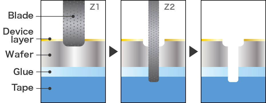
← Back to: Diamond Dicing Blades: The Complete Guide Kerf width — the width of material removed by the dicing blade — is one of the most important dimensional output ...
← Back to: Diamond Dicing Blades: The Complete Guide Kerf width — the width of material removed by the dicing blade — is one of the most important dimensional output ...
← Back to: Diamond Dicing Blades: The Complete Guide Blade loading is one of the most misdiagnosed failure modes in wafer dicing. Because its symptoms — rising chipping, increasing spindle ...
← Back to: Diamond Dicing Blades: The Complete Guide When a dicing blade wears out in half the expected service life, the instinct is often to blame the blade supplier. ...
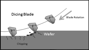
← Back to: Diamond Dicing Blades: The Complete Guide Chipping is the most common and yield-impacting defect in wafer dicing. A chip that appears to be within the die edge ...
← Back to: Diamond Dicing Blades: The Complete Guide QFN (Quad Flat No-Lead) package singulation presents a set of dicing challenges that are qualitatively different from wafer dicing. Instead of ...
← Back to: Diamond Dicing Blades: The Complete Guide Silicon carbide has become the substrate of choice for high-voltage power semiconductors driving electric vehicles, solar inverters, and industrial motor drives. ...
← Back to: Diamond Dicing Blades: The Complete Guide Blade dressing is one of the most important — and most often misunderstood — maintenance operations in wafer dicing. Done correctly, ...
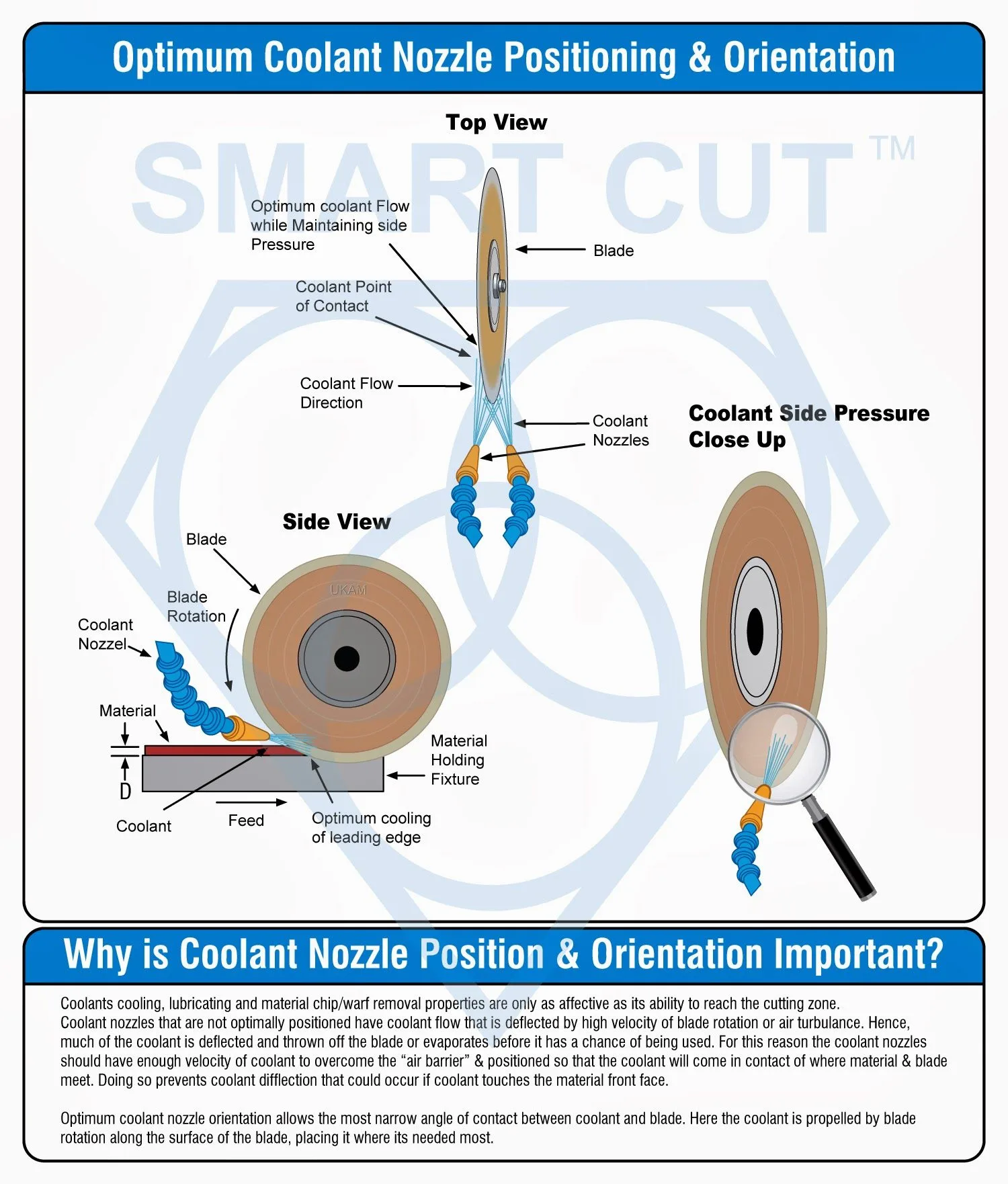
← Back to: Diamond Dicing Blades: The Complete Guide Deionised water is cheap, clean, and universally available — so why do semiconductor manufacturers formulate specialised coolant additives for dicing? Because ...
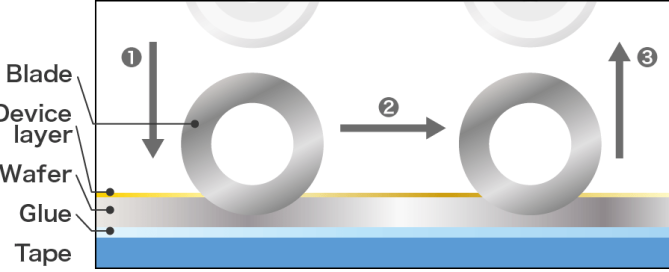
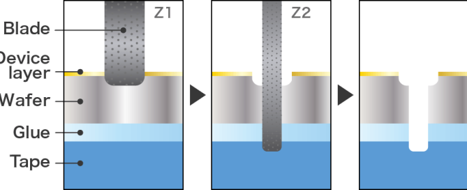
← Back to: Diamond Dicing Blades: The Complete Guide Wafer dicing — the process of singulating a finished wafer into individual die — sits at the intersection of mechanical precision, ...
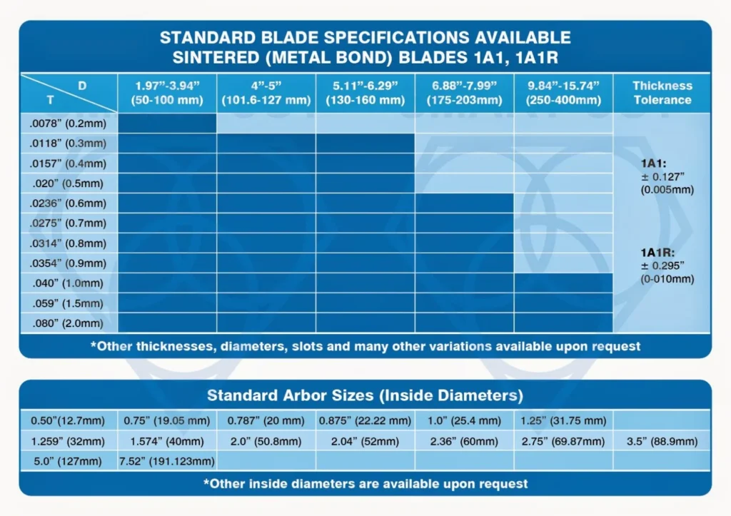
← Back to: Diamond Dicing Blades: The Complete Guide No single dicing blade specification works across all substrate materials. The mechanical properties of the workpiece — hardness, brittleness, fracture toughness, ...
High-Precision Surface Processing Materials
Polishing Slurries · Polishing Pads · Semiconductor Dicing Blades
Reliability and consistency for critical manufacturing steps.
Copyright ©2026 Wuxi Jizhi Electronic Technology Co., Ltd.
Phone
+(86) 180-6835-1533
contact@jeez-semicon.com
Address
Wuxi, Jiangsu, China


