logo

Acerca de semiconductor

Este autor aún no ha rellenado ningún dato.
Hasta ahora semiconductor ha creado 51 entradas de blog.

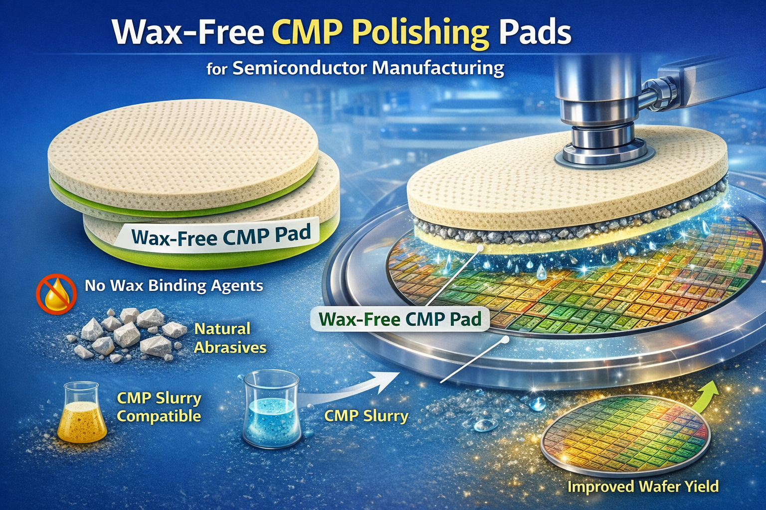
Explicación de los materiales y la estructura de las almohadillas de pulido CMP

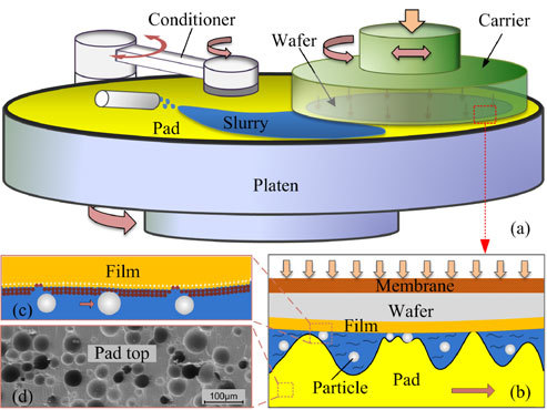
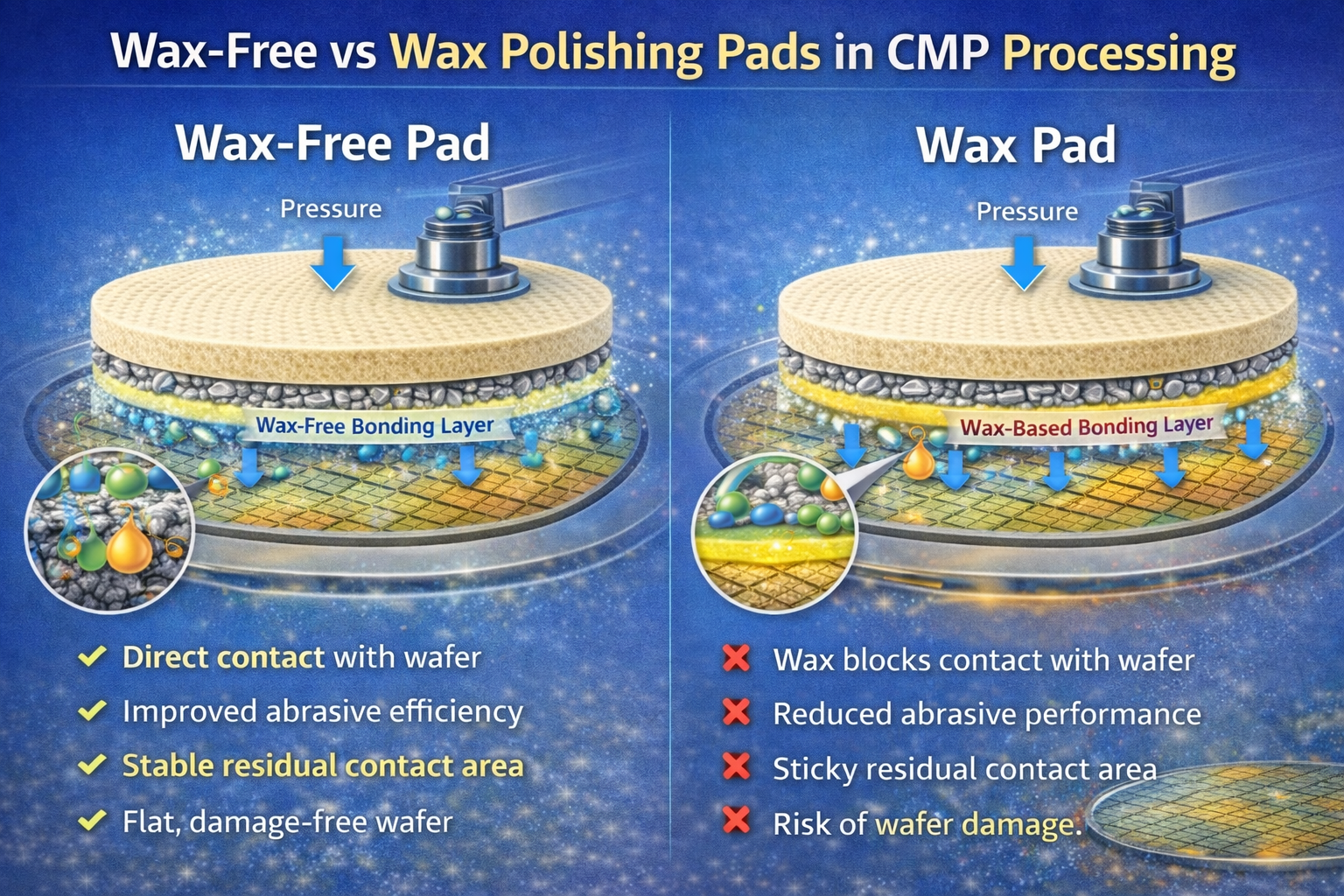
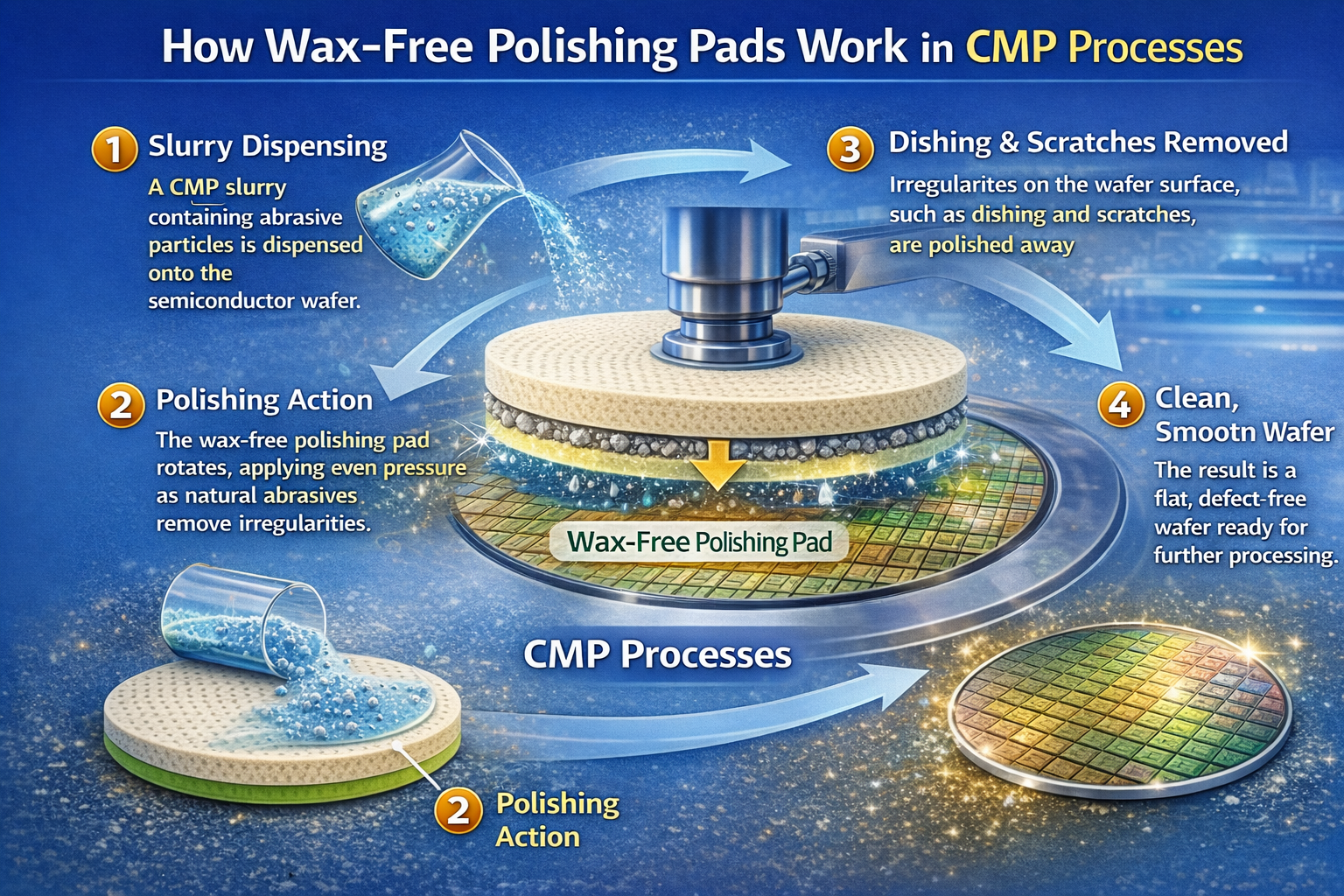
En CMP, los materiales de las almohadillas de pulido definen las interacciones mecánicas, químicas y tribológicas fundamentales que, en última instancia, determinan la eficacia de la planarización, la defectuosidad y la estabilidad del proceso. En el caso de las almohadillas de pulido CMP sin cera, la selección del material es aún más crítica porque la fijación de la oblea, la transmisión de la fuerza y la interacción de la lechada se rigen directamente por las propiedades de la superficie y el volumen de la almohadilla, en lugar de por las capas de cera auxiliares. Este documento proporciona un análisis a nivel de material y mecanismo de los materiales de las almohadillas de pulido CMP, centrándose en los sistemas de polímeros, el diseño microestructural, los parámetros mecánicos, el comportamiento de desgaste y sus implicaciones específicas para las arquitecturas de almohadillas sin cera. Tabla de contenidos Visión general de los materiales de las almohadillas de pulido CMP Química de polímeros y diseño de la matriz Microestructura y ...

Por |2026-01-12T10:54:52+08:002026E7416701265E5|Blog, Industria|0 Comentarios

Almohadillas de pulido sin cera en aplicaciones de proceso CMP

En la fabricación moderna de semiconductores, la CMP ya no es una operación unitaria aislada, sino un módulo de proceso estrechamente integrado que interactúa con la deposición previa, la limpieza posterior y la gestión general del rendimiento. La adopción de almohadillas de pulido CMP sin cera altera fundamentalmente la forma en que se sujetan, cargan, pulen y liberan las obleas, lo que requiere una integración deliberada del proceso en lugar de una simple sustitución de consumibles. Este documento se centra en cómo se integran en la práctica las almohadillas de pulido sin cera en los procesos CMP, qué parámetros del proceso se ven directamente afectados y cómo pueden aprovechar las fábricas las arquitecturas sin cera para mejorar la estabilidad del proceso, la uniformidad del rendimiento y la rentabilidad. Tabla de contenidos Integración de las almohadillas sin cera en el flujo CMP ...

Por |2026-01-12T10:53:59+08:002026E7416701265E5|Blog, Industria|0 Comentarios

Wax-Free vs Wax Polishing Pads in CMP Processing

In chemical mechanical planarization (CMP), the polishing pad is not merely a consumable surface but a critical process component that directly affects wafer flatness, material removal rate (MRR), defectivity, yield stability, and overall cost of ownership (CoO). Among available pad architectures, wax-free CMP polishing pads and traditional wax-based polishing pads represent two fundamentally different philosophies of wafer fixation, force transmission, and contamination control. This page provides an engineering-level comparison between wax-free and wax polishing pads, focusing on structural design, adsorption mechanisms, process behavior, defect risks, maintenance complexity, and long-term manufacturing economics. The goal is to support data-driven decision-making rather than ...

Por |2026-01-12T10:49:50+08:002026E7416701265E5|Blog, Industria|0 Comentarios

How Wax-Free Polishing Pads Work in CMP Processes

    Table of Contents 1. Introduction: Why Wax-Free Pad Working Principles Matter 2. CMP System Context: Wax-Free Pads as a Mechanical Subsystem 3. Pad–Wafer Contact Mechanics Without Wax Bonding 4. Wafer Loading and Initial Adsorption Formation 5. Pressure Ramp-Up and Adsorption Force Stabilization 6. Slurry Introduction and Frontside–Backside Decoupling 7. Steady-State CMP: Dynamic Adsorption Under Motion 8. Thermal and Mechanical Stability During CMP Operation 9. Controlled Wafer Release and De-Adsorption Behavior 10. Manufacturing-Level Process Control Implications 1. Introduction: Why Wax-Free Pad Working Principles Matter Understanding how wax-free polishing pads work is essential for modern CMP process development because wafer ...

Por |2026-01-12T10:42:02+08:002026E7416701265E5|Blog, Industria|0 Comentarios

Wax-Free Adsorption Polishing Pad Technology

  Table of Contents 1. Technology Overview: Adsorption as a Replacement for Wax Bonding 2. Fundamental Sources of Adsorption Force in Wax-Free Pads 3. Pad Microstructure Design and Adsorption Efficiency 4. Contact Mechanics at the Pad–Wafer Interface 5. Tunable Engineering Parameters Affecting Adsorption 6. Adsorption Stability Under CMP Operating Conditions 7. Adsorption Degradation and Failure Modes 8. Position of Adsorption Technology Within CMP Systems 1. Technology Overview: Adsorption as a Replacement for Wax Bonding Wax-free adsorption polishing pad technology was developed to eliminate the inherent limitations of wax-based wafer bonding in CMP. Traditional wax layers introduce viscoelastic behavior, thermal sensitivity, ...

Por |2026-01-12T10:48:33+08:002026E7416701265E5|Blog, Industria|0 Comentarios

Wax-Free CMP Polishing Pads for Semiconductor Manufacturing

  Table of Contents 1. Definition and Technical Scope of Wax-Free CMP Polishing Pads 2. Product Forms and Design Intent of Wax-Free Polishing Pads 3. Core Technology: Wax-Free Adsorption Fundamentals 4. How Wax-Free CMP Polishing Pads Work in Practice 5. Wax-Free vs Wax-Based CMP Polishing Pads 6. Integration of Wax-Free Pads in CMP Processes 7. Material and Structural Foundations of Wax-Free CMP Pads 1. Definition and Technical Scope of Wax-Free CMP Polishing Pads Wax-free CMP polishing pads are engineered wafer holding and polishing interfaces designed to operate without wax or adhesive bonding layers during chemical mechanical planarization. Unlike traditional wax-based ...

Por |2026-01-12T10:46:47+08:002026E7416701265E5|Blog, Industria|0 Comentarios

How to Choose CMP Slurry

  An Engineering-Level Decision Framework for Semiconductor Wafer Polishing Table of Contents 1. Introduction 2. First-Principles Approach to Slurry Selection 3. Wafer Material Considerations 4. Matching Slurry Type to CMP Process 5. Key Performance Metrics 6. Process Window & Margin Engineering 7. Compatibility with CMP Polishing Pads 8. Defectivity & Yield Risk Assessment 9. CMP Tool & Delivery System Constraints 10. High-Volume Manufacturing (HVM) Considerations 11. Common CMP Slurry Selection Mistakes 12. Qualification & Ramp-Up Strategy 13. Engineering Summary 1. Introduction Choosing the right CMP slurry is one of the most consequential decisions in semiconductor manufacturing. Unlike many consumables, slurry ...

Por |2026-01-05T16:34:14+08:002026年1月5日|Blog, Industria|0 Comentarios

CMP Slurry Filters

  Filter Media, Housing Design, and Point-of-Use Control in Semiconductor CMP Table of Contents 1. Overview of CMP Slurry Filters 2. Role of Filters in CMP Yield Control 3. Filter Media Materials 4. Absolute vs Nominal Rating 5. Pore Size Distribution & Cutoff Behavior 6. Filter Housing Design 7. Point-of-Use (POU) Filtration 8. Chemical Compatibility & Extractables 9. Performance Data & Lifetime Modeling 10. Failure Modes & Root Cause Analysis 11. HVM Filter Management Strategy 12. How to Select CMP Slurry Filters 13. Future Trends 1. Overview of CMP Slurry Filters CMP slurry filters are precision components designed to remove ...

Por |2026-01-05T16:28:13+08:002026年1月5日|Blog, Industria|0 Comentarios

CMP Slurry Filtration

  Particle Control, Yield Protection, and Process Stability in Semiconductor CMP Table of Contents 1. Introduction 2. Why Filtration Is Critical in CMP 3. Particle Sources in CMP Slurry Systems 4. Particle Size vs Defect Mechanisms 5. CMP Slurry Filter Technologies 6. Filter Pore Size Selection Strategy 7. Chemical Compatibility & Slurry Stability 8. Experimental Data & Filtration Performance 9. Filtration Process Window 10. Integration with CMP Tools 11. Filtration Failure Modes & RCA 12. HVM Filtration Strategy 13. Future Trends 1. Introduction CMP slurry filtration is one of the most underestimated yet yield-critical elements in semiconductor manufacturing. While slurry ...

Por |2026-01-05T16:25:16+08:002026年1月5日|Blog, Industria|0 Comentarios

Tungsten CMP Slurry for Semiconductor Manufacturing

  Table of Contents 1. Introduction to Tungsten CMP 2. Tungsten CMP Applications in Semiconductor Devices 3. Material Properties of Tungsten Relevant to CMP 4. Chemical–Mechanical Removal Mechanism 5. Tungsten CMP Slurry Composition Architecture 6. Chemical Kinetics & Rate-Limiting Steps 7. Engineering Parameters & Experimental Data 8. Process Window & Control Maps 9. Defect Mechanisms & Root Cause Analysis 10. High-Volume Manufacturing Challenges 11. Slurry Selection & Optimization Guidelines 12. Future Trends in Tungsten CMP Slurry 1. Introduction to Tungsten CMP Tungsten Chemical Mechanical Planarization (CMP) plays a critical role in semiconductor manufacturing, particularly for contact plug and via fill ...

Por |2026-01-05T16:19:16+08:002026年1月5日|Blog, Industria|0 Comentarios
Ir arriba