logo

Acerca de semiconductor

Este autor aún no ha rellenado ningún dato.
Hasta ahora semiconductor ha creado 62 entradas de blog.

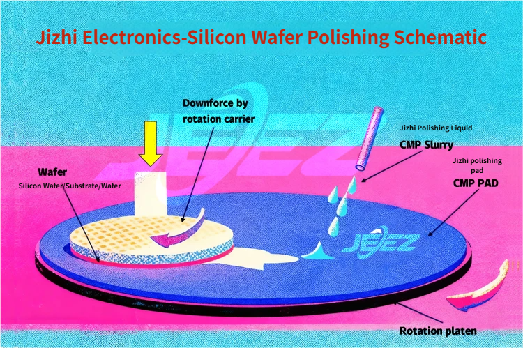
Analysis of Key Polishing and Lapping Processes for InP (Indium Phosphide) Substrates

Indium Phosphide (InP), as a core material of the third-generation semiconductor, holds an irreplaceable position in high-end fields such as optical communications, millimeter-wave radar, and quantum communications due to its ...

Por |2025-12-25T10:48:50+08:0020255E7412670565E5|Blog, Industria|0 Comentarios

La “revolución de las superficies” en la fabricación de semiconductores: La esencia técnica y el valor fundamental del pulido de obleas de silicio

In the precision manufacturing chain of the semiconductor industry, the creation of every high-performance chip relies on hundreds of process steps, from silicon purification to chip packaging. Among these, silicon ...

Por |2025-12-05T11:01:27+08:0020255E7412670565E5|Blog, Industria|0 Comentarios

Superar el elevado coste y la lentitud de respuesta del G804W

As the third-generation semiconductor industry accelerates its iteration today, silicon carbide (SiC), as a core material, is reshaping the technological landscape of high-end manufacturing fields such as new energy vehicle ...

Por |2025-12-05T10:57:18+08:0020255E7412670565E5|Blog, Industria|0 Comentarios

Desvelando los secretos de la lechada de pulido de vidrio óptico en los procesos CMP

Unlocking CMP Process: Principles and Advantages In the field of optical component processing, Chemical Mechanical Polishing (CMP) is a core technology for achieving high-precision surface planarization. Through the synergistic effects ...

Por |2025-12-05T10:50:44+08:0020255E7412670565E5|Blog, Industria|0 Comentarios

Producto 3C Solución para pulido de espejos: Lechada de pulido de sílice SiO2 sin picaduras

Why Choose CMP Over Electrochemical Polishing for 3C Product Mirror Polishing? In the 3C industry (mobile phones, laptops, smart wearables, etc.), electrochemical polishing is gradually being replaced by CMP (Chemical ...

Por |2025-12-25T10:47:48+08:0020255E7412670565E5|Blog, Dinámica|0 Comentarios

Funciones y eficacia de la suspensión diamantada (especializada para el pulido CMP)

In fields such as semiconductor manufacturing, precision optics, and hard alloy processing, the ultra-precision polishing of material surfaces directly determines product performance and reliability. Leveraging advanced R&D capabilities and mature ...

Por |2025-12-05T10:34:39+08:0020255E7412670565E5|Blog, Dinámica|0 Comentarios

Lechada de pulido CMP para obleas de silicio electrónicas

I. CMP Polishing Technology: A Key Process in Semiconductor Manufacturing Chemical Mechanical Planarization (CMP) is one of the core processes in semiconductor silicon wafer manufacturing, directly impacting chip performance and ...

Por |2025-12-05T10:32:18+08:0020255E7412670565E5|Blog, Dinámica|0 Comentarios

Características y guía de selección del lodo para pulido de obleas CMP

In the global planarization stage of wafer manufacturing, Chemical Mechanical Polishing (CMP) is a critical process. As a core consumable, CMP polishing slurry directly determines key wafer surface metrics such ...

Por |2025-12-05T10:29:53+08:0020255E7412670565E5|Blog, Dinámica|0 Comentarios

Pulido espejo de cerámica de alúmina con pasta de pulido

Achieving a mirror finish on alumina ceramic sheets presents significant challenges for two main reasons: first, the high hardness of alumina makes it difficult to grind; second, its strong light-absorbing ...

Por |2025-12-16T11:46:18+08:0020255E7412670565E5|Aplicación|0 Comentarios
Ir arriba