CMP Materials: The Complete Guide for Semiconductor Engineers & Procurement Teams
Everything you need to know about Chemical Mechanical Planarization consumables — from fundamental process science to advanced-node slurry selection, polishing pad technology, supplier evaluation, and total cost of ownership optimization.
1. What Are CMP Materials?
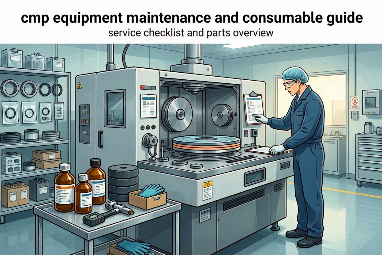
CMP materials - abréviation de Chemical Mechanical Planarization materials — are the consumable and semi-durable components that make the CMP process possible in semiconductor wafer fabrication. The term encompasses three major product categories: CMP slurries (polishing liquids containing chemical agents and abrasive particles), CMP polishing pads (the textured polymer surfaces against which wafers are polished), and CMP pad conditioners (diamond-dressed discs or brushes that restore pad surface texture).
Together, these materials must work in precise synchrony to remove excess material from a wafer’s surface and produce a globally flat topology — accurate to within a few nanometers — before the next lithographic layer is deposited. Without high-quality CMP consumables, the tight overlay budgets required by sub-10 nm process nodes simply cannot be met.
At JEEZ (Jizhi Electronic Technology Co., Ltd.), we supply precision CMP slurries and CMP polishing pads to fabs, research institutions, and equipment OEMs worldwide. Our product lines are engineered to support technology nodes from mature 28 nm platforms to the most demanding sub-5 nm and 3D-IC architectures.
2. Why CMP Is Critical in Semiconductor Fabrication
Modern integrated circuits are built layer by layer through a process known as the Front-End-of-Line (FEOL) and Back-End-of-Line (BEOL) sequence. Each layer introduces new topographic features — transistors, isolation trenches, metal interconnects, dielectric films — and every one of those features creates height variation on the wafer surface.
Left uncorrected, this growing surface topography would quickly exceed the depth-of-focus of advanced lithography tools, causing focus errors, CD (critical dimension) variation, and ultimately yield loss. CMP is the only wafer-level process capable of achieving the global planarization needed to reset surface height variation before the next lithographic patterning step.
Beyond planarization, CMP also serves as a material removal step in processes like copper damascene interconnect formation, STI (Shallow Trench Isolation), tungsten via fill, and high-k metal gate integration. In each case, the combination of chemical etching and mechanical abrasion removes overburden material with layer-specific selectivity — stopping precisely at the target film interface.
Key Process Steps Where CMP Is Essential
- STI (Shallow Trench Isolation): Removes excess SiO₂ deposited over trenches, stopping on the silicon nitride hard mask.
- ILD (Inter-Layer Dielectric) planarization: Flattens deposited oxide layers between metal routing tiers.
- Tungsten (W) CMP: Clears tungsten overburden after via fill, exposing the TiN barrier and dielectric.
- Copper (Cu) CMP: A two-step process removing bulk copper then the underlying barrier metals (Ta/TaN, TiN, or Co).
- Cobalt (Co) CMP: Increasingly used for advanced contact and local interconnect in sub-7 nm nodes.
- Polysilicon & Gate CMP: Used in gate-last HKMG integration schemes.
- Bonding layer planarization (3D-IC / wafer bonding): Achieves sub-0.3 nm roughness for direct dielectric bonding.
The breadth of these applications explains why CMP consumables must cover an enormous performance envelope — from aggressive oxide removal at multi-hundred nm/min rates, to ultra-gentle final polishing where a few nanometers of dishing or erosion can ruin a device.
3. How the CMP Process Works
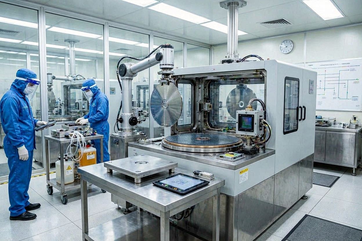
The CMP tool — often called a polisher or planarizer — consists of a rotating platen onto which the polishing pad is mounted, a wafer carrier (polishing head) that holds the wafer face-down, and a slurry delivery arm that dispenses fresh slurry at a controlled flow rate. The wafer and platen rotate, often at different speeds and in the same direction, while a controlled downforce is applied through the carrier.
Slurry delivery: Fresh slurry containing abrasive particles and chemical agents is dispensed onto the pad surface. The slurry is drawn under the wafer by pad rotation, forming a thin hydrodynamic film between the wafer and the pad asperities.
Chemical softening: Active chemical agents in the slurry react with the wafer surface material, forming a softer, more mechanically compliant oxide or hydroxide layer that is more easily abraded than the original film.
Mechanical abrasion: Abrasive particles — typically ceria (CeO₂), colloidal silica (SiO₂), or alumina (Al₂O₃) — physically remove the chemically modified surface layer. This combined action is what produces planarization rather than simple etching.
Material transport: Spent slurry, removed particles, and reaction by-products are carried away from the polishing interface by slurry flow and pad grooves, preventing re-deposition or scratch-inducing agglomeration.
Endpoint detection: Modern CMP tools monitor friction torque, optical reflectance (ISRM), or eddy-current signals to detect the moment the target removal depth is reached, then automatically stop or transition to the next polishing step.
Post-CMP clean: Wafers undergo immediate brush-scrub and megasonic cleaning to remove residual slurry particles and metal ions before entering the next process step. Post-CMP clean chemistry is tightly coupled to the slurry chemistry used.
The material removal rate (MRR) is governed by the Preston equation: MRR ∝ P × V, where P is the applied pressure (downforce per unit area) and V is the relative velocity between wafer and pad. In practice, modern multi-zone carriers allow independent pressure control across the wafer, compensating for edge effects and wafer bow to achieve ±1–2% within-wafer uniformity.
4. CMP Slurry — Types, Composition & Selection
CMP slurry is the most performance-critical consumable in the planarization process. It is a carefully engineered aqueous colloidal suspension containing abrasive particles, pH-controlling buffer agents, oxidizers, complexing agents, corrosion inhibitors, surfactants, and sometimes film-forming additives. Each chemical component serves a specific role in achieving the desired removal rate, selectivity, planarity, and defect performance.
Choosing the wrong slurry — or using the right slurry under poorly controlled conditions — is one of the most common root causes of CMP yield loss. Understanding slurry chemistry in depth is therefore foundational for any process engineer or procurement professional working with CMP consumables. Our detailed guide on CMP Slurry Types, Applications & Selection provides a comprehensive deep-dive; the key concepts are summarized below.
4a. Slurry Types by Application
| Slurry Type | Target Film(s) | Primary Abrasive | Key Chemistry | Process Step |
|---|---|---|---|---|
| Oxide / STI Slurry | SiO₂ (TEOS, HDP) | Ceria (CeO₂) | Alkaline, low ionic strength | STI, ILD planarization |
| Copper Bulk Slurry | Cu (overburden) | Silice colloïdale | H₂O₂ oxidizer, BTA inhibitor, organic acid complexant | Cu damascene Step 1 |
| Barrier / Clearing Slurry | Ta, TaN, TiN, Co, Ru | Colloidal silica or alumina | Moderate pH, selective etch formulation | Cu damascene Step 2 |
| Tungsten (W) Slurry | W, TiN | Alumina or colloidal silica | H₂O₂ / Fe-based oxidizer, acidic pH | W plug / via CMP |
| Cobalt (Co) Slurry | Co, Co barrier metals | Silice colloïdale | pH 4–7, mild oxidizer, Co-complexant | Advanced contact / BEOL |
| Polysilicon Slurry | Poly-Si, SiN | Silice colloïdale | Alkaline, high Si:SiN selectivity | Gate CMP, FEOL |
| Bonding Layer Slurry | SiO₂, SiCN | Ultra-pure colloidal silica | Near-neutral pH, very low particle concentration | Hybrid bonding (3D-IC) |
4b. Abrasive Chemistry: Ceria vs. Silica vs. Alumina
The choice of abrasive particle is arguably the single most important formulation decision in slurry design, as it determines both the material removal mechanism and the defect risk profile.
Ceria (CeO₂)
- Superior oxide removal rate due to chemical tooth effect
- High SiO₂:Si₃N₄ selectivity — ideal for STI
- Lower particle load needed → fewer defects at equivalent MRR
- Sensitivity to ionic contamination; requires tight bath control
- Higher raw material cost vs. silica
Silice colloïdale (SiO₂)
- Excellent particle uniformity and size control (20–120 nm)
- Low defectivity — preferred for copper, barrier, and bonding CMP
- Stable over broad pH range (2–12)
- Lower MRR than ceria at equivalent particle loading
- Most versatile abrasive; widest application range
Alumine (Al₂O₃)
- High hardness (Mohs 9) → aggressive metal removal
- Standard for tungsten CMP; effective for sapphire substrate polish
- Higher scratch risk on soft films; careful pH control essential
- Available in fumed and calcined crystal forms
- Less common in advanced logic; still widely used in compound semiconductors
Specialty Abrasives
- Zirconia (ZrO₂): Optical glass and ophthalmic lens polishing
- Diamond slurry: SiC substrate and GaN epi-layer planarization
- Mn-doped ceria: Next-gen low-defect oxide CMP at advanced nodes
- Coated particles: Core-shell designs for tunable selectivity
To learn how these abrasives perform specifically in advanced-node applications — including their interaction with novel metal films like ruthenium and molybdenum — see our detailed guide on CMP Materials for Advanced Nodes.
4c. How to Choose the Right CMP Slurry
Slurry selection involves balancing a set of competing performance targets. There is no universally “best” slurry — the optimal product is always process-specific. The critical parameters to evaluate include:
- Material Removal Rate (MRR): Target MRR is set by throughput requirements and overburden thickness. Too low and cycle time suffers; too high and endpoint control becomes unreliable.
- Selectivity: The ratio of removal rates between the target film and underlying stop layer (e.g., Cu:barrier, SiO₂:Si₃N₄). Higher selectivity gives greater process latitude.
- Within-Wafer Uniformity (WIWNU): Radial MRR variation across a 300 mm wafer; best-in-class slurries achieve <2% 1σ.
- Defectivity: Scratch count, particle count, and metal contamination levels as measured by surface inspection tools (KLA, Hitachi).
- Dishing & Erosion: Over-polishing artifacts that remove material from within features or pattern-dense areas.
- Stability & Shelf Life: Slurry particle size distribution must remain stable throughout storage and in-tool pot life.
- Post-CMP Clean Compatibility: The slurry’s chemistry must be removable with available brush-scrub and megasonic clean chemicals.
For guidance on safe handling, storage temperature requirements, shelf-life best practices, and disposal regulations for CMP slurries, see our dedicated resource on Stockage, manutention et sécurité des boues CMP.
5. CMP Polishing Pads — Technology & Selection
The CMP polishing pad is the second pillar of the CMP consumable system. It provides the mechanical polishing surface that contacts the wafer and also serves as a slurry transport medium, carrying fresh slurry into the contact zone and removing reaction by-products. Pad selection has a profound influence on removal rate, within-wafer uniformity, defect levels, and pad lifetime.
Most commercial CMP pads are made from polyurethane — chosen for its chemical resistance, tuneable mechanical properties, and well-understood pore structure. Pad microstructure, surface texture, macro-geometry (diameter, thickness, groove pattern), and bulk viscoelastic properties collectively determine polishing performance. For a comprehensive technical breakdown of pad technologies, refer to our in-depth article on CMP Polishing Pads: Technologies & Comparison.
5a. Pad Types: Hard, Soft & Stacked
Hard Pads (IC1000-type)
- Closed-cell polyurethane foam, Shore D hardness 50–65
- High planarization efficiency — removes step height quickly
- Industry standard for oxide, W, and barrier CMP
- Lower contact conformity to local wafer topography
- Requires frequent conditioning to maintain MRR
Soft Pads (Politex-type)
- Felt-based or open-cell foam; Shore A hardness 15–30
- Conformal contact → lower defectivity, lower scratch count
- Used as second-step (buff) pads after bulk removal
- Limited planarization efficiency for high topography
- Preferred for copper buff and final SiO₂ smooth-out
Stacked / Composite Pads
- Hard top pad laminated onto a compressible sub-pad
- Sub-pad compliance compensates for wafer bow
- Combines planarization efficiency with edge uniformity
- Most widely used configuration in high-volume manufacturing
- Sub-pad material (PE foam, Suba) selected for compressibility
Fixed Abrasive Pads (FAP)
- Abrasive particles embedded in pad matrix — no separate slurry required
- Exceptional uniformity for post-STI and optical-grade polishing
- Used in sapphire, SiC, and certain glass substrate applications
- Higher consumable cost; limited to specific applications
- Emerging interest for advanced wafer bonding preparation
5b. Key Pad Properties That Affect Performance
Understanding these physical parameters allows engineers to make informed pad selection decisions and troubleshoot process issues more effectively:
| Propriété | Gamme typique | Effect on Process |
|---|---|---|
| Hardness (Shore D) | 40–65 (hard); 15–30 (soft) | Higher hardness → more planarization; lower hardness → lower defects |
| Porosity (%) | 20–60% | More porous → better slurry retention; lower MRR stability long-term |
| Pore diameter (μm) | 20–80 μm | Affects slurry transport volume and pad-wafer real contact area |
| Groove pattern | Concentric, X-Y, radial, perforated | Controls macro slurry distribution; affects WIWNU at wafer edge |
| Compressibility | 0.5–5% | Higher compressibility → better uniformity on bowed wafers |
| Storage modulus (E’) | Frequency-dependent | Viscoelastic response determines pad behavior at high platen speed |
| Surface asperity height | 20–80 μm (conditioned) | Contact area with wafer; declining asperity = glazing = MRR drop |
5c. Pad Conditioning & Lifetime Management
CMP pads do not maintain a constant surface state during polishing. The mechanical and chemical environment of the process progressively smooths the pad surface asperities — a phenomenon called vitrage à plots — which reduces the effective contact area between pad and wafer and causes MRR to decline. Conditionnement des tampons restores the pad surface by abrading a fresh micro-texture using a diamond-embedded conditioning disc.
Two conditioning modes are used in production:
- In-situ (concurrent) conditioning: The conditioner operates simultaneously with wafer polishing. Maintains stable MRR but increases pad wear rate and cost of ownership.
- Ex-situ conditioning: Pad is conditioned between wafer runs. Lower pad wear, but MRR may drift within a run if the conditioning interval is too long.
Conditioner design, diamond grit size, conditioner downforce, sweep pattern, and conditioning time all interact with pad and slurry to determine the steady-state MRR and pad life. For a full technical treatment of conditioner selection and process optimization, see our guide on Conditionneurs de tampons CMP et processus de conditionnement.
6. CMP Materials for Advanced Nodes (Below 14 nm)
The transition from planar transistors to FinFET and now Gate-All-Around (GAA) nanosheet architectures has fundamentally changed the demands placed on CMP consumables. As device features shrink below 10 nm and 3D stacking (3D NAND, HBM, 3D-IC) becomes mainstream, CMP processes must operate with tighter removal budgets, lower defect densities, and compatibility with an expanding menu of exotic materials.
Our full technical resource on CMP Materials for Advanced Nodes (Below 14 nm) covers these challenges in detail. Key themes are summarized here:
Novel Metal Films Requiring New CMP Chemistries
Advanced logic nodes are introducing metals beyond the traditional Cu/W/Ti/Ta system. Each new material requires a purpose-engineered slurry chemistry:
- Cobalt (Co): Used for local interconnects and contacts in 7 nm and below; requires slurries that balance Co removal against underlying dielectric erosion without inducing galvanic corrosion at Co/TiN interfaces.
- Ruthenium (Ru): A leading candidate to replace W in contacts and local interconnects at sub-5 nm due to lower resistivity at small dimensions; Ru CMP chemistry is still maturing.
- Molybdenum (Mo): Gaining attention as an alternative liner metal and gate fill material for GAA devices; requires strongly oxidizing acidic slurries.
- High-k dielectrics (HfO₂, ZrO₂, La₂O₃): CMP of high-k gate dielectrics requires very low and controllable removal rates to avoid dielectric thinning.
3D-IC and Wafer Bonding Planarization
Hybrid bonding — where two wafers are joined through direct dielectric-to-dielectric and metal-to-metal contact — demands post-CMP surface roughness below 0.3 nm Ra and near-zero surface particle contamination. These requirements are far beyond those of conventional CMP and require:
- Ultra-dilute, ultra-pure colloidal silica slurries with narrow particle size distributions
- Soft polishing pads with high conformity and minimal defect generation
- Extended post-CMP clean processes using SC1/SC2 or dilute HF sequences
CMP Step Count Trends
Advanced logic wafers now undergo 30 to 60+ CMP steps per wafer by the time they reach final metallization. This dramatic increase — versus fewer than 10 steps in 180 nm processes — means that marginal improvements in per-step defect density, uniformity, and consumable consistency have compounding effects on overall yield and cost.
7. Common CMP Defects and How to Prevent Them
CMP-related defects account for a significant fraction of yield-impacting events in semiconductor fabs. Understanding the root causes of each defect type — and the levers available to reduce them — is essential for process engineers at every node. Our comprehensive article on Défauts du processus CMP : Causes, types et solutions provides the full engineering treatment.
| Defect Type | Primary Cause | Affected Process | Prevention Strategy |
|---|---|---|---|
| Scratches | Oversized particles, agglomerated abrasives, pad debris | All CMP steps | Slurry filtration, particle size control, pad inspection |
| La pêche | Over-polishing of metal within wide features | Cu, W, Co CMP | Endpoint control, slurry selectivity optimization |
| Erosion | Thinning of dielectric in dense pattern areas | Cu CMP Step 2, oxide CMP | Slurry selectivity tuning, pattern density normalization |
| Corrosion / Pitting | Galvanic corrosion, aggressive slurry pH | Cu CMP, Co CMP | BTA or azole inhibitors, pH optimization |
| Delamination | Excessive downforce on low-k dielectric films | Ultra-low-k CMP | Reduced downforce, soft pads, elastic modulus matching |
| Residual particles | Incomplete post-CMP clean | All CMP steps | Optimize brush-scrub chemistry, megasonic frequency |
| Metal contamination | Metal ion leaching from slurry or pad | FEOL, gate CMP | Ultra-pure materials, post-CMP SC1/DHF clean |
Many of these defects are interrelated. For example, increasing slurry oxidizer concentration to improve copper removal rate also increases the risk of corrosion pitting — requiring a corresponding adjustment of inhibitor concentration. Effective defect management therefore requires a systems-level approach to the slurry–pad–process parameter interaction space.
8. Evaluating CMP Materials Suppliers
The CMP materials supply chain is highly concentrated at the top tier — a handful of global manufacturers supply the majority of volume to leading-edge fabs. However, the competitive landscape has broadened significantly over the past decade, with capable regional suppliers and technology-focused challengers offering strong alternatives for many application categories.
Our side-by-side analysis in the article Top CMP Materials Suppliers: 2026 Comparison profiles the major players across slurry, pad, and conditioner segments. When evaluating any CMP materials supplier, the following criteria should be applied systematically:
Supplier Evaluation Framework
Technical Capability
- Product coverage across your specific process nodes and materials
- In-house R&D and application engineering resources
- Availability of application-specific qualification data
- Track record at leading-edge nodes (<7 nm)
- Ability to develop custom formulations
Quality & Consistency
- Lot-to-lot particle size distribution variability (CV <5% preferred)
- Certified purity levels for critical metal impurities (<ppb)
- ISO 9001 / IATF certification; SEMI S2 / S8 compliance
- Transparent COA (Certificate of Analysis) issuance
- Shelf life and stability data under shipping conditions
Supply Chain Reliability
- Geographic manufacturing footprint relative to your fab location
- Safety stock and lead-time commitments
- Single-source vs. dual-source raw material strategy
- Business continuity and disaster recovery planning
- Export compliance and regulatory status
Total Cost of Ownership
- Unit price vs. effective cost per wafer pass
- Consumable lifetime and pad/slurry consumption per wafer
- Tool qualification cost and timeline
- Technical support and field application engineering fees
- Waste disposal and environmental compliance costs
JEEZ maintains manufacturing and application engineering capabilities across Asia, with global logistics to serve fabs in North America, Europe, and Southeast Asia. Our slurries and polishing pads are qualified on major CMP tool platforms including Applied Materials Mirra / Reflexion, Ebara FREX, and KCTECH KU series systems.
9. CMP Materials Market Outlook 2026–2030
The global CMP consumables market entered 2026 on strong footing following a recovery cycle driven by AI accelerator chip demand, HBM memory expansion, and the ramp of advanced logic nodes at leading-edge fabs. Our full analysis is covered in the article Marché des matériaux CMP : Tendances et perspectives 2025-2030.
Key market drivers in 2026: AI training hardware (H100/B200-class GPUs and custom ASICs) requires advanced packaging with extensive CMP steps for TSV planarization and redistribution layer formation. High-Bandwidth Memory (HBM3 and HBM3E) stacking increases the number of CMP-intensive wafer bonding steps per device. Meanwhile, the 2 nm GAA node ramp at TSMC, Samsung, and Intel Foundry is pulling through new demand for Ru, Co, and Mo-compatible slurry chemistries.
Supply Chain and Geopolitical Considerations
Export controls on semiconductor manufacturing equipment and materials — particularly from the United States and Japan — have accelerated localization efforts for CMP consumables in China and other regions. Fabs operating under supply-chain constraints are actively diversifying their supplier bases, creating opportunities for qualified regional suppliers who can meet the technical demands of advanced-node production.
Rare earth supply security is also a factor: ceria (CeO₂) abrasive production is concentrated in China, which accounts for the vast majority of global cerium oxide output. Fabs and slurry formulators are exploring synthetic ceria production routes, ceria-free oxide slurry alternatives, and strategic inventory buffers to manage supply risk.
10. In-Depth Topic Guides
This pillar page provides a comprehensive overview of CMP materials. Each of the specialized topics below has its own dedicated guide, where our engineering team goes substantially deeper into the technical details, process data, and selection criteria. Explore the topics most relevant to your current project:
11. Frequently Asked Questions
What is CMP slurry made of?
CMP slurry is an aqueous suspension containing abrasive particles (most commonly ceria, colloidal silica, or alumina), a pH-buffering agent, an oxidizer (such as hydrogen peroxide for copper slurries), chemical complexants or chelating agents, corrosion inhibitors, and surfactants. The exact formulation varies significantly by application — oxide slurries, copper slurries, and tungsten slurries each have distinct chemistries optimized for their target film and process requirements.
What is the difference between CMP and dry etching?
Dry etching (plasma etch, RIE) is an anisotropic material removal process that selectively removes material in a directional pattern defined by a lithographic mask. CMP is a global, isotropic material removal process that acts on the highest topographic points first, progressively reducing height variation until the wafer surface is flat. CMP does not require a lithographic mask and is used specifically for planarization and bulk material removal, not for pattern formation.
How do I choose between a hard and a soft CMP pad?
Hard pads are preferred when global planarization efficiency is the priority — they make contact predominantly with the highest topographic points and remove them faster than the lower areas. Soft pads are preferred when defect minimization and surface finish quality are the priority, such as in copper buff polishing or final oxide smoothing. Most advanced production CMP processes use a stacked pad configuration (hard top pad + compressible sub-pad) to balance planarization and uniformity simultaneously.
What causes scratching in CMP, and how is it prevented?
Scratching is most commonly caused by large or agglomerated abrasive particles in the slurry, pad debris, or contaminant particles introduced through the slurry distribution system. Prevention measures include point-of-use filtration of the slurry at 0.1–1 μm cut-off, regular inspection and cleaning of slurry lines, tight particle size distribution control during slurry manufacturing, and monitoring of conditioner disc integrity to prevent diamond shard release.
How long does a CMP polishing pad last?
Pad lifetime varies widely depending on the application, tool platform, conditioning program, and pad type. In high-volume manufacturing, hard pads used for oxide CMP typically last 500–2,000 wafer passes before replacement. Soft buff pads used for copper CMP may last longer due to gentler process conditions. Pad lifetime is determined by monitoring MRR stability, within-wafer-non-uniformity trends, and periodic pad thickness measurement. Most fab process engineers set a conservative replacement trigger to maintain process stability well before true pad failure.
What are the environmental and safety considerations for CMP slurries?
CMP slurries contain a range of chemical agents with varying hazard profiles. Oxidizers such as hydrogen peroxide are reactive and must be stored away from organics. Metal-containing slurries (particularly those with iron-based catalysts or copper ions from recirculated bath chemistry) require careful handling to prevent skin and eye exposure and must be disposed of as hazardous waste in compliance with local regulations. All JEEZ slurry products come with a comprehensive Safety Data Sheet (SDS) and storage recommendations. Detailed guidance is available in our guide on Stockage, manutention et sécurité des boues CMP.
Can CMP materials be used for compound semiconductor substrates (GaAs, SiC, GaN)?
Yes, but specialized formulations are required. SiC substrates — used for power electronics and EV inverters — require alkaline colloidal silica slurries with oxidizing agents, or diamond-abrasive slurries in final stages, due to the extreme hardness of SiC (Mohs 9.5). GaN epi-layers require carefully controlled slurry pH and abrasive hardness to avoid subsurface damage that would degrade device mobility. GaAs polishing uses bromine-methanol or HNO₃/HF-based chemistries in addition to mechanical abrasion. JEEZ offers application-specific advice for compound semiconductor customers — contactez notre équipe technique for a consultation.
How does CMP fit into 3D-IC and chiplet integration?
CMP plays an increasingly central role in advanced packaging. In Through-Silicon Via (TSV) processes, CMP removes copper overburden above the via openings and performs final planarization before bonding. In hybrid bonding for 3D-IC stacking (as used in HBM and advanced logic-on-logic integration), CMP must achieve sub-nanometer surface roughness on both oxide bonding surfaces to enable void-free room-temperature direct bonding. These requirements demand the highest-performance slurries and pads available and represent a fast-growing area of CMP materials development.
Ready to Optimize Your CMP Process?
JEEZ application engineers work directly with process teams to select, qualify, and optimize CMP slurries and polishing pads for your specific tool, node, and throughput requirements. Whether you are qualifying a new process at a leading-edge node or looking to reduce consumable cost at a mature technology platform, we have the product portfolio and expertise to support you.
Contact a JEEZ CMP Expert