Planarization in Semiconductor Manufacturing: The Complete 2026 Guide
Semiconductor planarization is one of the most process-critical techniques in modern chip fabrication. Without it, every layer added to a wafer would inherit and amplify the topographic irregularities of all layers below — making advanced lithography, via formation, and multi-layer interconnects physically impossible. This complete 2026 guide covers everything: the physics that makes planarity essential, the techniques that deliver it, the consumables that define its performance, and the frontier challenges shaping its next decade.
01What Is Semiconductor Planarization?
Semiconductor planarization is the process of creating a flat, highly uniform surface on a silicon wafer during the sequential steps of integrated circuit (IC) manufacturing. At its core, it solves a geometrically inevitable problem: as devices are built layer by layer through repeated cycles of deposition, patterning, and etching, the surface topography of the wafer grows with every processing step. Individual device features — gate stacks, contact plugs, metal lines, and dielectric films — each contribute raised regions and recessed trenches that accumulate into a progressively more irregular landscape.
Left uncorrected, this growing surface roughness and topographic variation would make every subsequent process step less reliable, less uniform, and ultimately non-functional. Planarization is the intervention that resets the surface, restoring the flatness required for the next layer to be deposited and patterned with precision.
Local vs. Global Planarization
A foundational distinction in understanding planarization is the difference between local and global effectiveness. These two categories define not just the scale of flatness achieved, but which planarization techniques are appropriate for which process applications:
- Local planarization reduces surface step heights over short lateral distances — typically in the range of a few micrometers to tens of micrometers. It may smooth out the profile directly adjacent to an individual device feature without improving long-range variation across the chip or the wafer. Spin-on-Glass (SOG), BPSG thermal reflow, and resist etch-back all fall in this category.
- Global planarization achieves surface uniformity across the full chip area (several cm²) and, critically, across the entire wafer diameter — typically 300 mm in high-volume manufacturing. Only global planarization satisfies the depth-of-focus requirements of modern immersion and EUV lithographic exposure systems. Chemical Mechanical Planarization (CMP) is currently the only production-viable technique that reliably achieves true global planarization.
The Topography Problem in Practice
Consider a simple example: a transistor gate stack, 80 nm tall, is patterned and formed on the silicon surface. A 500 nm inter-layer dielectric (ILD) oxide is then deposited by CVD over it. The oxide film largely conforms to the shape of the underlying features, leaving a step height at the gate edge. An aluminum or copper interconnect line is then deposited and patterned — and it too inherits this topology, creating a step at its edge. By the time the third or fourth metal layer is reached, the cumulative step height from all layers below can easily exceed 300–500 nm across the chip.
Modern photolithographic exposure systems operating at 193 nm immersion have a depth-of-focus window as small as ±50 nm. EUV lithography at 3 nm and below demands even tighter surface tolerances. Any surface variation greater than this window — anywhere within the chip exposure field — causes dimensional errors in the printed pattern that translate into transistor and interconnect defects.
Deep dive: What Is Semiconductor Planarization? Definition, History & Why It Matters →02Why Planarization Is Critical in Modern IC Fabrication
The necessity of planarization is not constant — it scales in urgency and technical demand with every generation of transistor shrink and interconnect complexity increase. A chip from the 1980s with a single aluminum metal layer, 2 µm feature sizes, and generous depth-of-focus could absorb substantial surface variation without catastrophic yield loss. The situation as of June 2026 is categorically different.
A leading-edge logic chip at the 2 nm node contains over 100 billion transistors and may incorporate 15 or more metal interconnect layers stacked above the device tier. Each layer is built upon the surface established by the one below it. If planarization is skipped or inadequate at any module, the consequences compound through all subsequent process steps.
Key Failure Modes Without Adequate Planarization
Lithographic Focus Failure
Optical lithography systems have a finite depth-of-focus window. At 193 nm immersion lithography — the backbone of production nodes from 45 nm through 7 nm — this window can be as narrow as ±50 nm. EUV lithography, standard at 3 nm and below, is similarly unforgiving. Surface height variations beyond this range cause the aerial image to fall out of focus over portions of the exposure field, producing critical dimension (CD) errors that directly degrade transistor performance uniformity across the die and across the wafer.
Via Fill Incompleteness
Chemical vapor deposition of tungsten (W) or electrochemical deposition of copper (Cu) into contact holes and vias is highly sensitive to the depth and geometry of the entry surface. On a non-planar substrate, hole depths vary across the chip depending on the underlying topography, producing inconsistent fill levels — some contacts underfilled (creating resistance hotspots), others potentially bridging adjacent structures.
Barrier Metal Continuity Failure
Thin barrier layers — TaN and Ta for copper interconnects, TiN for tungsten — are deposited at thicknesses of just 3–10 nm. When deposited over topographic step edges on an un-planarized surface, these thin films develop mechanical stress concentrations that can lead to electromigration failures, leakage paths, or delamination during device operation — critical reliability concerns in any advanced BEOL stack.
Cumulative Topography Amplification
Without planarization at each major integration module, step heights accumulate additively across the full device stack. In a 15-layer interconnect stack without inter-level CMP, the upper metal layers may encounter surface variations of several hundred nanometers — exceeding the process window of any deposition, etch, or lithography tool in the facility.
03The Evolution of Planarization Technology
Semiconductor planarization has a history spanning over six decades, with each era defined by the process challenge of the prevailing node and the innovation that addressed it.
1961 — The Wafer Polish
Bob Walsh at Monsanto Company adapted optical glass polishing techniques to single-crystal silicon, developing the use of colloidal silica slurry to remove saw damage from freshly sliced silicon wafers before device fabrication. This chemo-mechanical polishing approach — applying an abrasive, chemically reactive liquid to a rotating surface — established the physical principles that would define CMP a generation later. For two decades, however, the technique remained confined to raw wafer preparation only.
1970s–1980s — Spin-on-Glass and BPSG Reflow
As bipolar and early CMOS devices added multiple levels of polysilicon and aluminum metallization, engineers deployed two chemical planarization approaches for the inter-level dielectric (ILD). Spin-on-Glass (SOG) — solutions of silicon alkoxide precursors spun onto wafers and thermally cured — deposited thin, relatively planar oxide films. Borophosphosilicate Glass (BPSG), a phosphorus- and boron-doped oxide, could be thermally reflowed at 850–950°C to level individual step heights via viscous flow. Both provided local planarization only, and the high reflow temperatures became increasingly incompatible with advanced metallization as aluminum was replaced by refractory and then copper-based conductors.
1988–1990 — The CMP Breakthrough
IBM’s process integration teams identified that achieving global planarization — the kind required for sub-micron optical lithography — demanded a fundamentally different approach. Their solution: pressing a process wafer face-down against a rotating pad wetted with a chemically reactive abrasive slurry. The first technical publication describing this technique for in-process device wafers appeared in 1988. Within two years, the approach had been proven capable of true global planarity and was entering production development.
1997 — Copper CMP Enables Damascene Interconnects
IBM’s introduction of copper damascene interconnects in production at Burlington, Vermont required a CMP step to remove copper overburden and expose the inlaid lines — the first commercial “metal CMP” application. This copper CMP process cemented the technology’s role as irreplaceable in BEOL processing and drove the rapid development of copper-compatible slurry chemistries and low-defect polishing consumables.
2000s–2020s — From STI to FinFET
STI CMP became the standard isolation technique for CMOS logic; tungsten plug CMP defined contact formation; ILD CMP multiplied as metal layer counts grew from 3 to 8 to 12. The emergence of high-k/metal gate processes, FinFET architecture, and replacement metal gate (RMG) flows added new CMP modules. By the early 2020s, a leading-edge logic chip required 15–20 individual CMP steps.
2025–2026 — Advanced Nodes and New Materials
As of June 2026, Gate-All-Around (GAA) nanosheet transistors, 3D IC hybrid bonding, SiC power device fabrication, and extreme uniformity requirements at 2 nm logic nodes represent the current frontier of planarization engineering. The number of CMP steps per chip has exceeded 25 at leading nodes, and entirely new chemistries are being developed for materials — SiC, GaN, ruthenium — that conventional silicon CMP slurries cannot address.
Full timeline: What Is Semiconductor Planarization? Definition, History & Why It Matters →04Planarization Techniques: A Comprehensive Overview
Before Chemical Mechanical Planarization became the dominant approach, the semiconductor industry developed and refined a range of planarization techniques. Understanding these methods — and why each falls short of the global planarization that advanced nodes require — provides essential context for why CMP has become indispensable.
The single most important classification axis is local vs. global planarization. Local methods reduce step heights near individual features but leave long-range wafer-scale variation intact. Global planarization achieves uniformity across the full chip area and wafer diameter — the only standard compatible with sub-100 nm optical lithography.
Major Semiconductor Planarization Techniques Compared
| Technique | Mechanism | Planarity Scale | Primary Application | Key Limitation |
|---|---|---|---|---|
| BPSG Thermal Reflow | Viscous flow at 850–950°C | Local | Pre-metal dielectric (PMD) | High temperature budget; incompatible with advanced metallization |
| Spin-on-Glass (SOG) | Liquid-phase spin + thermal cure | Local | Early ILD planarization | Thin effective thickness; cracks in thick deposits; limited gap fill |
| Resist Etch-Back | Blanket photoresist coat + RIE etch | Local–Moderate | ILD leveling at 0.5–1 µm nodes | Pattern-density dependent; complex endpoint; not fully global |
| HDP-CVD | Simultaneous deposition + sputter etch | Modéré | STI gap fill; dielectric fill | Geometry-dependent; not true global planarization |
| Electrochemical Planarization (ECP) | Selective electrochemical removal | Local | Copper film leveling (pre-CMP) | Applicable to conductive surfaces only; not stand-alone global |
| Chemical Mechanical Planarization (CMP) | Simultaneous chemical + mechanical removal | Global ✓ | All major IC planarization modules | Complex consumable management; requires post-CMP cleaning step |
CMP achieves global planarization through a mechanism none of the other techniques possess: the compliant polishing pad contacts the wafer surface across its full diameter simultaneously, and the removal rate at any point is proportional to the local contact pressure. Elevated surface features, which protrude into the pad and experience higher contact stress, are polished away faster than recessed areas. This self-leveling behavior — governed by Preston’s equation — drives the entire surface toward a common plane, regardless of the initial pattern density or step height distribution.
Earlier techniques like SOG and BPSG reflow are still encountered in legacy device manufacturing (200 mm fabs, power devices, MEMS), and HDP-CVD remains standard for STI gap filling prior to CMP. But for critical global planarization steps, CMP has been the uncontested standard since the mid-1990s.
Full comparison: Semiconductor Planarization Techniques — CMP vs. SOG vs. Etch-Back →05CMP: How It Works — The Industry Standard
Chemical Mechanical Planarization is the simultaneous application of chemical reactivity and mechanical abrasion to remove material from a wafer surface and converge it toward global planarity. The defining characteristic of CMP is that neither the chemistry nor the mechanics alone produces global planarization — it is their synergistic combination that makes the process uniquely effective.
The Physics: Preston’s Equation
The governing relationship for CMP material removal rate (MRR) was first described by Frank Preston in 1927 in the context of optical glass polishing, and remains the foundational model for CMP process development today:
MRR = Kp × P × V
Where Kp is the Preston coefficient (a material- and slurry-specific constant), P is the contact pressure between the pad and wafer surface, and V is the relative velocity between wafer and pad. Because elevated surface features experience higher local contact pressure than recessed areas, they are removed faster — producing the self-leveling behavior that enables global planarization.
Key CMP Hardware Components
A production CMP system consists of four primary elements working in concert:
- Rotary platen: A large (600–700 mm diameter) rigid stainless steel or granite disk that holds the polishing pad and drives its rotation at controlled speeds (typically 50–150 rpm).
- Polishing pad: A polyurethane foam pad affixed to the platen surface. Its hardness, porosity, groove pattern, and surface texture determine how slurry is distributed and how uniformly contact pressure is applied across the wafer.
- Carrier head (wafer chuck): Holds the wafer face-down against the rotating pad. Applies controlled down-force (typically 1–6 psi), and may apply differential back-pressure to specific wafer zones through multiple chambers to compensate for within-wafer non-uniformity.
- Slurry delivery system: Dispenses the chemical slurry at controlled flow rates (100–300 mL/min) onto the pad surface. Point-of-use filtration and temperature control are critical for particle size distribution stability.
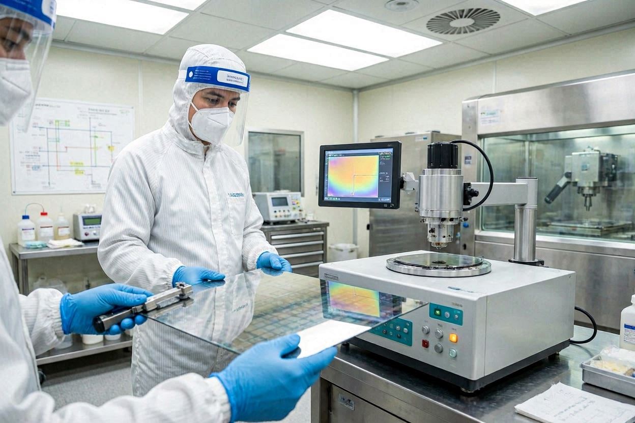
The CMP Process: Seven Critical Steps
Pre-CMP Metrology
The wafer’s incoming film thickness and surface topography are measured by optical reflectometry, spectroscopic ellipsometry, or capacitance-based mapping. This data informs the polishing recipe — setting target removal depth, down-force profile, and endpoint detection thresholds.
Pad Conditioning
A diamond-embedded conditioning disk dresses the pad surface, restoring the open-pore microstructure and asperity height needed for effective slurry transport and mechanical contact. Conditioning can occur in-situ (simultaneously with wafer polishing) or ex-situ (between wafers). The conditioning rate directly controls pad wear rate and process stability.
Livraison de boues
The chemical slurry — an aqueous dispersion of nano-scale abrasive particles in a reactive carrier — is pumped at controlled temperature and flow rate onto the rotating pad surface. The slurry fills pad pores and is distributed across the polishing interface by pad rotation and groove geometry.
Polissage
The carrier head lowers the wafer face-down onto the rotating pad. Applied down-force (1–6 psi), carrier and platen rotational speeds, and carrier sweep oscillation frequency are all independently controlled. Abrasive particles in the slurry mechanically abrade the wafer surface while chemical agents simultaneously react with and soften the target film, dramatically increasing removal rate beyond what either mechanism alone could achieve.
Chemical Reaction at the Interface
Slurry chemistry is specifically formulated to react with the target film. For copper CMP, H₂O₂ oxidizes Cu to Cu₂O, which is mechanically softer and more easily abraded. For oxide CMP, alkaline chemistry breaks Si–O surface bonds, facilitating material removal. For tungsten CMP, oxidizing agents form a brittle WO₃ surface layer. In each case, the chemistry lowers the effective hardness of the surface, enabling abrasive particles to remove material efficiently without excessive pad wear.
Endpoint Detection (EPD)
The system monitors polishing progress in real time. Optical EPD uses interferometry or reflectometry to detect fringe pattern changes as film thickness decreases. Motor current EPD detects changes in friction torque as a harder stop layer is reached. Eddy-current sensors can measure copper film thickness in-situ. When the target endpoint is reached, polishing is stopped automatically to prevent over-polish.
Post-CMP Cleaning
Immediately after polishing, the wafer undergoes brush scrubbing, megasonic cleaning, and wet chemical rinse to remove residual slurry particles, metallic contaminants, and organic residues before the next process step. This is a mandatory quality-determining step, not an optional finishing step.
06CMP Slurry: The Chemical Engine of Planarization
CMP slurry is the active medium through which both the chemical reactivity and the abrasive force that drive material removal are delivered to the wafer surface. It is a precisely engineered aqueous dispersion whose composition — abrasive particle type, particle size distribution, oxidizer concentration, pH, surfactants, and chelating agents — must be tuned specifically to the target film, the required removal rate, and the selectivity between the film being removed and the stop layer below it.
Slurry Composition: The Four Core Components
1. Abrasive Particles
Nano-scale particles (typically 20–200 nm in diameter) dispersed in the aqueous carrier provide mechanical cutting action at the pad–wafer interface. The three principal abrasive materials used in semiconductor CMP are:
- Colloidal silica (SiO₂): Manufactured by controlled hydrolysis of tetraethyl orthosilicate (TEOS), producing spherical particles with narrow size distributions and smooth surfaces. Used for oxide ILD polishing, copper CMP final buff, and silicon finishing. Produces very low surface roughness (Ra < 0.3 nm) due to soft abrasion. pH stable in alkaline conditions (pH 9–11).
- Fumed ceria (CeO₂): Provides dramatically higher oxide removal rates than silica through the “chemical tooth” mechanism — Ce³⁺/Ce⁴⁺ redox cycling at the CeO₂ surface breaks Si–O–Si bonds chemically, supplementing mechanical abrasion. Achieves oxide-to-nitride selectivity of 50:1 to over 100:1, making it the preferred abrasive for STI CMP where precise stopping on Si₃N₄ is essential.
- Fumed alumina (Al₂O₃): High Mohs hardness (9) and sharp particle morphology provide aggressive material removal. Standard for tungsten (W) CMP applications. Care must be taken to minimize surface defects through process optimization.
2. Oxidizing Agents
React with the metal surface to form a chemically softer oxide or hydroxide layer that is more readily abraded by the slurry particles. Hydrogen peroxide (H₂O₂) is the dominant oxidizer for copper CMP; KIO₃ and H₂O₂ are used for tungsten CMP. Oxidizer concentration must be carefully controlled — too low produces inadequate MRR; too high can lead to excessive film dissolution or re-deposition.
3. Complexing and Chelating Agents
Organic compounds such as glycine, ammonium citrate, and benzotriazole (BTA) stabilize dissolved metal ions in solution (preventing re-deposition as particles), or form passivation layers on metal surfaces to control dissolution selectivity between features and field regions. In copper CMP, BTA concentration directly controls the dishing rate on wide copper features.
4. Surfactants and pH Buffers
Surfactants control the colloidal stability of abrasive particles (preventing agglomeration), modify surface wetting, and influence the adsorption of chemical species at the wafer surface. pH buffers maintain the required chemical environment (typically pH 4–6 for copper CMP, pH 10–11 for oxide CMP) throughout the polishing process.
CMP Slurry Families by Application
| Slurry Type | Primary Abrasive | Gamme de pH | Film cible | Key Selectivity |
|---|---|---|---|---|
| Oxide ILD CMP | Colloidal SiO₂ | 10–11 | TEOS SiO₂, USG | SiO₂ >> Si₃N₄ |
| STI CMP | Fumed CeO₂ | 5–7 | HDP-CVD SiO₂ | SiO₂ : Si₃N₄ > 50:1 |
| Tungsten (W) CMP | Fumed Al₂O₃ | 2-4 | CVD W plug | W : SiO₂ ~ 5–10:1 |
| Copper (Cu) CMP | Colloidal SiO₂ | 4–6 | ECD Cu damascene | Cu > TaN barrier > SiO₂ |
Slurry stability — the ability of particles to remain uniformly dispersed over time and under the mechanical stresses of pumping and dispense — is a critical quality parameter. Abrasive agglomeration produces large clusters that cause surface scratching defects, a major yield loss mechanism in CMP. This makes point-of-use filtration, temperature control, use-by management, and mixing protocol essential disciplines in any CMP operation.
Complete guide: CMP Slurry for Semiconductor Planarization — Chemistry, Types & Selection →07CMP Polishing Pads: The Mechanical Foundation
The polishing pad is the physical interface between the CMP platen and the wafer surface. Its mechanical properties — hardness, compressibility, surface texture, and groove geometry — fundamentally determine how uniformly the slurry is distributed, how contact pressure is applied across the wafer, and ultimately how well global planarization is achieved. Pad selection is as important to process performance as slurry selection; the two consumables must be engineered as a system.
Pad Structure and Classification
The vast majority of production CMP pads are manufactured from polyurethane foam, selected for its controlled hardness, resistance to slurry chemistry, and the ability to engineer porosity and surface texture with precision.
Two-Layer Stacked Pads (Standard Production)
The most widely used configuration in leading-edge logic and memory fabs:
- Hard top layer (e.g., IC1000 equivalent): A rigid, microporous polyurethane foam with a grooved surface. The hardness (Shore D ~60) provides the rigidity needed for global planarization — soft pads conform to surface topography and lose the self-leveling advantage. Micropores store and transport slurry to the polishing interface. Groove patterns (concentric rings, radial, X-Y grid, or spiral) are precision-machined to ensure uniform slurry distribution and prevent slurry hydroplaning at high rotational speeds.
- Soft bottom layer (e.g., SUBA equivalent): A compressible felt or open-cell foam sublayer affixed below the hard layer. It provides mechanical cushioning and compliance, absorbing platen run-out and enabling the pad stack to conform to wafer-scale bow (typically ±30–80 µm for 300 mm wafers), distributing contact pressure more uniformly across the full wafer diameter.
Fixed Abrasive Pads
Specialty pads in which abrasive particles (typically CeO₂ or Al₂O₃) are embedded directly into the pad matrix in a controlled distribution. Used without conventional slurry (or with a slurry-free chemistry), they offer superior defect performance for applications where conventional slurry contamination is a concern, such as post-STI and advanced copper buff.
Pad Conditioning: Maintaining Polishing Consistency
Over time, the pad surface becomes glazed — polishing debris fills the micropores, and the surface asperities (micro-scale protrusions that abrade the wafer) flatten and round under repeated mechanical loading. A glazed pad delivers dramatically reduced material removal rate and degraded within-wafer uniformity, making pad conditioning a continuous and critical process control step.
A diamond-embedded conditioning disk — a metal disk with precisely distributed CVD diamond crystals — is pressed against the rotating pad surface to continuously abrade away the glazed top layer and restore the open-pore, high-asperity surface texture. The conditioning aggressiveness (disk force, relative velocity, sweep pattern) is balanced against pad wear life: too aggressive shortens pad life and changes the pad properties over time; too mild allows glazing and uniformity drift.
Detailed analysis: CMP Polishing Pads — Types, Structure & Role in Wafer Planarization →08Planarization Applications in IC Fabrication
CMP is deployed at every major integration module in the IC fabrication process flow. Each application has distinct objectives, specific film systems, unique selectivity requirements, and characteristic defect modes that process engineers must understand and control. The four primary CMP applications — STI, ILD, copper damascene, and tungsten plug — together account for the majority of CMP tool utilization in any leading-edge fab.
Shallow Trench Isolation (STI) CMP
Shallow trenches (200–400 nm deep) are etched into the silicon substrate, filled with HDP-CVD oxide, and the oxide overburden is removed by CMP to leave the isolation oxide level with the silicon surface. Ceria-based slurries achieve oxide-to-nitride selectivity ratios of 50:1 to over 100:1, stopping precisely on the Si₃N₄ hard mask. WIWNU in STI CMP directly determines isolation oxide thickness uniformity, which affects transistor threshold voltage distribution across the chip.
Inter-Level Dielectric (ILD) CMP
Between each metal interconnect layer (M1 through M15+ in advanced logic), a thick SiO₂ or low-k dielectric film is deposited by CVD and then planarized by CMP to remove all step height from the metal layer below. Oxide CMP slurries (colloidal silica, alkaline chemistry) are standard. Post-CMP oxide thickness uniformity is typically specified at ±5–10 nm across the 300 mm wafer — a WIWNU of <2%.
Copper Damascene CMP
After copper electroplating fills dual-damascene trenches and vias, a two-step CMP process removes the copper overburden (Step 1: high-rate Cu removal) and then the TaN/Ta barrier metal (Step 2: endpoint-controlled). The principal defect modes are dishing (over-polishing of wide Cu features) and erosion (thinning of dielectric in dense pattern arrays). Slurry BTA concentration, down-force, and flow rate are the primary control knobs.
Tungsten (W) Plug CMP
After W-CVD fills contact holes and deposits a thick field overburden, CMP removes the W and TiN/TiW barrier on the inter-layer dielectric, leaving filled contact plugs flush with the dielectric surface. Al₂O₃ slurry with H₂O₂ oxidizer is standard. The challenge is achieving uniform removal across contacts of varying density, size, and proximity to the die edge without over-polishing the surrounding oxide.
Additional CMP Applications in Advanced Process Flows
Replacement Metal Gate (RMG) CMP
In high-k/metal gate processes used at 22 nm and below, a dummy polysilicon gate is removed after source/drain formation and replaced with a high-k dielectric and low-resistance metal gate stack. The CMP step that planarizes the inter-layer dielectric to expose the dummy gate top for removal — and then the subsequent step that planarizes the metal gate fill — are both critical for gate height uniformity and effective work function control.
Through-Silicon Via (TSV) Reveal CMP
In 3D stacked memory and logic packages, TSVs fabricated from the front side must be revealed by thinning the wafer back-side down to the copper TSV tips. A TSV reveal CMP step removes the bulk silicon and polishes the back-side surface until the copper plugs are uniformly exposed, with minimal dishing of the copper relative to the silicon field.
Hybrid Bonding Planarization
In die-to-die hybrid bonding for 3D IC integration, the bonding surface of each die must be polished to an Ra below 0.3 nm with copper-to-dielectric step heights of less than 2–3 nm. This represents among the most extreme surface specifications in any area of semiconductor manufacturing, and requires dedicated planarization tools and consumables engineered specifically for this application.
Module-by-module guide: Planarization Applications in IC Fabrication — STI, ILD, Cu Damascene & W Plug →09Planarization at Advanced Technology Nodes
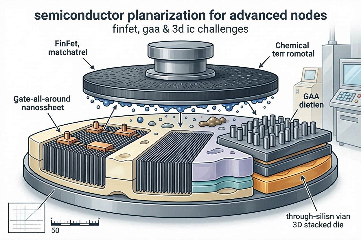
As logic technology advances from FinFET at 7 nm through Gate-All-Around (GAA) nanosheet at 3 nm and 2 nm, the requirements placed on every planarization step become dramatically more stringent — in uniformity, defect density, step height control, and material compatibility with new gate dielectrics, contact metals, and low-k dielectric systems.
FinFET Planarization (14 nm – 5 nm)
FinFET devices require STI CMP to define the silicon fin height with precision and uniformity across the full 300 mm wafer. The fin height — determined by how much silicon stands above the recessed STI oxide after CMP — directly controls the transistor’s on-current (Ion). A fin height variation of ±2 nm across the chip translates into measurable transistor performance spread and die-to-die variation.
This places WIWNU requirements on STI CMP at the sub-1% level across the full 300 mm wafer — a specification that demands both excellent CMP tool hardware (multi-zone carrier head pressure control) and precisely formulated high-selectivity ceria slurry. The Replacement Metal Gate (RMG) process adds a second demanding CMP application: planarization of the ILD to expose the dummy gate, and then planarization of the deposited high-k/metal gate stack — both with tight height uniformity specifications tied directly to gate work function and threshold voltage control.
GAA Nanosheet Planarization (3 nm – 2 nm)
The transition from FinFET to Gate-All-Around (GAA) nanosheet transistors — now in high-volume production or advanced development at leading logic foundries as of June 2026 — introduces entirely new CMP requirements. Nanosheet channel formation requires the uniform removal of SiGe sacrificial layers from alternating Si/SiGe stacks. The process demands extremely high Si-to-SiGe selectivity to preserve the nanosheet channel thickness (typically 5–7 nm) while removing all SiGe material. A polishing non-uniformity of just 1 nm across the wafer is significant relative to the 5–7 nm channel.
Leading-edge 2 nm / equivalent-node logic chips now require more than 25 individual CMP steps across the full FEOL and BEOL process flow — covering STI, ILD, tungsten contacts, copper BEOL layers (up to 15 levels), replacement metal gate, nanosheet formation, and self-aligned contact modules. Each step carries its own uniformity budget that contributes to the overall chip yield equation.
3D NAND Memory Planarization
Multi-layer 3D NAND flash memory structures stack 96, 128, 176, or more alternating oxide/nitride layers above the silicon substrate. The cumulative topography from step-and-repeat depositions of these thin-film stacks must be periodically corrected by CMP before high-aspect-ratio channel hole etching, whose depth uniformity is critically sensitive to the incoming surface flatness. The specific challenge in 3D NAND CMP is maintaining uniformity across extremely pattern-dense arrays while preventing the development of “center-to-edge” doming effects in the thick multilayer stack.
Advanced Packaging: Hybrid Bonding
In die-to-wafer and wafer-to-wafer hybrid bonding for 3D IC integration, the bonding interface is prepared by CMP to achieve surface roughness below Ra 0.3 nm and copper pad protrusion (or recess) below 2–3 nm relative to the surrounding dielectric. The mechanism of hybrid bonding — direct Cu-to-Cu metallic bonding and SiO₂-to-SiO₂ oxide fusion bonding simultaneously — requires both surfaces to be atomically clean, ultra-smooth, and geometrically matched at the sub-nanometer level. Any surface contamination, particle, or step height exceeding specification prevents void-free bonding and creates electrical resistance at the Cu-Cu interface.
In-depth analysis: Semiconductor Planarization for Advanced Nodes — FinFET, GAA & 3D IC Challenges →10SiC & Wide Bandgap Semiconductor Planarization
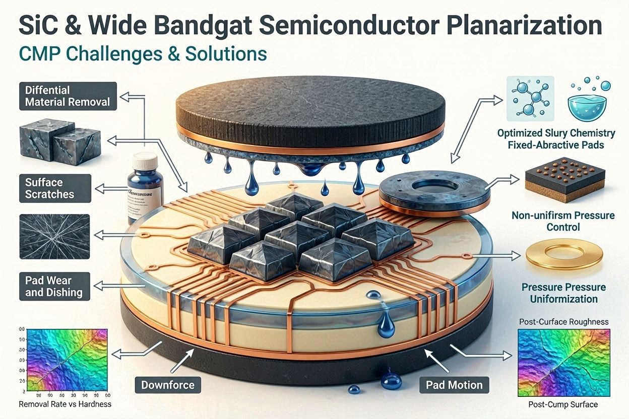
The rapid growth of the power semiconductor market — driven by electric vehicle inverters, industrial motor drives, and renewable energy power conditioning — has elevated silicon carbide (SiC) and other wide bandgap (WBG) materials from niche to mainstream. Planarizing these substrates presents challenges fundamentally different from silicon CMP, driven by the same exceptional materials properties that make WBG devices attractive for high-voltage, high-temperature operation.
Why SiC Planarization Is Technically Demanding
Silicon carbide has a Mohs hardness of approximately 9.2–9.5, placing it among the hardest known materials — far above silicon (6.5) and alumina (9.0). Its chemical stability, which makes it resistant to corrosion in harsh environments, also makes it extremely resistant to the wet chemical dissolution mechanisms that drive silicon CMP. The result is material removal rates (MRR) 10–50× lower than comparable silicon oxide CMP, making throughput a significant economic constraint for SiC device manufacturers.
SiC also presents a structural asymmetry: the Si-face (0001) and C-face (000-1) of a SiC wafer have significantly different surface chemistries and oxidation rates under identical polishing conditions. The C-face is substantially more reactive, producing non-uniform polishing across a wafer that has both faces exposed or in multi-wafer batch processes.
Advanced CMP Chemistries for SiC
Emerging SiC CMP approaches exploit advanced oxidation chemistry to improve MRR while maintaining the ultra-low roughness (Ra < 0.2 nm) required for subsequent epitaxial layer growth. Two approaches are under active development and early production deployment as of June 2026:
- Fenton-type chemistry: H₂O₂ combined with Fe²⁺ catalyst generates highly reactive hydroxyl radicals (·OH) at the slurry–SiC interface. These radicals rapidly oxidize the SiC surface to a thin, soft SiO₂ layer that is easily abraded by colloidal silica particles, effectively decoupling the mechanical and chemical removal rates. MRR improvements of 3–5× over conventional alkaline silica CMP have been reported.
- KMnO₄-based oxidizing slurries: Potassium permanganate provides strong oxidizing power at moderate temperatures, forming MnO₂ and SiO₂ surface films on SiC. Compatible with near-neutral pH chemistry, reducing equipment corrosion concerns compared to strongly alkaline or acidic alternatives.
GaN-on-Si and GaN-on-SiC substrates for RF and power electronics applications face similar CMP challenges: high hardness, chemical stability, and cleavage anisotropy all complicate the development of manufacturable planarization processes.
Full technical guide: SiC & Wide Bandgap Semiconductor Planarization — CMP Challenges & Solutions →11Post-CMP Cleaning & Planarization Metrology
The CMP process inherently introduces surface contamination — residual slurry particles, metallic ions from the polished film and slurry chemistry, and organic residues from surfactants and chelating agents. Post-CMP cleaning is therefore a mandatory process step in every CMP module, not an optional finishing step. The wafer’s cleanliness and surface quality after post-CMP cleaning directly determines the yield of the next deposition, etch, or lithography step.
Post-CMP Cleaning Methods
PVA Brush Scrubbing
Polyvinyl alcohol (PVA) brush rollers — cylindrical sponge brushes with precisely controlled pore size and hardness — make gentle mechanical contact with the wafer front and back surfaces simultaneously, dislodging slurry particles through a combination of mechanical action and surface tension gradients in the rinse liquid. PVA brush cleaning is performed in the presence of dilute chemical solutions: deionized water (DIW), 0.1–1% citric acid for metal contamination control, or dilute NH₄OH for particle removal. It is the most common first cleaning step after CMP.
Megasonic Cleaning
High-frequency acoustic waves (typically 850 kHz to 2 MHz) applied to a chemical bath (SC1: NH₄OH/H₂O₂/H₂O, or DIW) generate microstreaming and acoustic pressure gradients at the wafer surface that dislodge particles without direct mechanical contact. Effective for removing particles from high-aspect-ratio surface features — topographic valleys or narrow trenches — that brush scrubbing cannot access.
Wet Chemical Cleaning (RCA-based)
Sequential chemical baths address the different contamination types: SC1 (NH₄OH:H₂O₂:H₂O = 1:1:5 at 65–75°C) removes organic contamination and many particles; SC2 (HCl:H₂O₂:H₂O = 1:1:6) removes residual metals. For copper CMP, dilute citric acid is often used in place of SC2 to avoid chloride-induced corrosion of the exposed copper surface.
Planarization Metrology: Key Parameters
Surface Roughness
Post-CMP surface roughness is characterized by atomic force microscopy (AFM) over representative scan areas (typically 5×5 µm to 50×50 µm). Key roughness metrics include: Ra (arithmetic average of absolute height deviations from mean, typically specified as <0.5 nm for advanced logic CMP); Rq (root mean square roughness, more sensitive to occasional high-amplitude features); and Rz (maximum peak-to-valley height over the measurement area, relevant for defect-density-limited applications like hybrid bonding).
Film Thickness and Uniformity
WIWNU (Within-Wafer Non-Uniformity) is the standard metric for planarization quality: the standard deviation of residual film thickness measured across a defined matrix of points on the wafer, expressed as a percentage of the mean thickness. Leading-edge CMP processes target WIWNU <1%. TTV (Total Thickness Variation) — the full range (maximum minus minimum) of film thickness across the wafer — provides a complementary worst-case measure of flatness.
Endpoint Detection Review
Post-process metrology (reflectometry, ellipsometry, or four-point probe for metal films) validates the in-situ endpoint detection result and provides the data feedback needed for run-to-run process control systems (R2R control) that adjust the next wafer’s polishing recipe based on the current lot’s results.
Complete guide: Post-CMP Cleaning & Planarization Metrology — Ensuring Surface Quality →12JEEZ CMP Solutions for Semiconductor Planarization
Jizhi Electronic Technology Co., Ltd. — operating under the JEEZ brand at jeez-semicon.com — is a direct manufacturer of CMP consumables for semiconductor planarization applications. As a manufacturer rather than a distributor, JEEZ maintains full control over product formulation, quality, and technical support, enabling rapid qualification cycles and responsive customization for specific process requirements.
CMP Polishing Slurries
JEEZ offers a comprehensive portfolio of CMP polishing slurries engineered for oxide ILD, STI, tungsten plug, and copper damascene planarization. Products are available in both colloidal silica and ceria abrasive formulations, with application-matched chemical packages optimized for the target film system’s removal rate, selectivity, and surface finish requirements. JEEZ slurries are formulated with tight particle size distribution control and long-term stability to minimize agglomeration risk and support extended slurry management windows in high-volume manufacturing environments.
CMP Polishing Pads
JEEZ CMP polishing pads are engineered in single-layer and two-layer stacked configurations covering ILD, STI, tungsten, and copper CMP applications. Hard polyurethane top layers with optimized groove patterns ensure uniform slurry distribution and consistent material removal rates. All pads are validated for chemical compatibility with the full range of JEEZ slurry products, as well as interoperability with third-party consumable systems.
Absorption and Backing Films
JEEZ supplies absorption and backing films for CMP carrier head assemblies. These films provide precise wafer retention, uniform pressure distribution, and consistent carrier head performance run-over-run — a foundational element of achieving tight WIWNU specifications in production environments.
All JEEZ products are manufactured under ISO-certified quality management systems and are available for qualification at logic, memory, power device, and compound semiconductor fabs worldwide. JEEZ engineering support teams work directly with fab process engineers to accelerate slurry and pad qualification, providing detailed process characterization data and application-specific recommendations.
Ready to Optimize Your CMP Process?
Contact the JEEZ technical team to request product datasheets, discuss slurry and pad qualification requirements, or get application-specific recommendations for your planarization process modules.
Get in Touch with JEEZ →FAQQuestions fréquemment posées
Semiconductor planarization is the process of creating a flat, highly uniform surface on a silicon wafer during integrated circuit (IC) fabrication. As each layer of material is deposited and patterned, surface topography accumulates across the wafer. Left uncorrected, these height variations cause lithographic focus failures, via fill defects, and barrier metal discontinuities in subsequent layers. Chemical Mechanical Planarization (CMP) — which combines abrasive slurry chemistry with mechanical polishing action — is the dominant technique for achieving global planarization across the full wafer diameter, a prerequisite for reliable advanced-node manufacturing.
CMP is the only production-viable technique that achieves global planarization — uniform flatness across the entire chip area and wafer diameter. Earlier methods like Spin-on-Glass (SOG), BPSG reflow, and resist etch-back deliver only local planarization, reducing step heights near individual features without correcting long-range wafer-scale variation. CMP’s self-leveling mechanism (governed by Preston’s equation: MRR = Kp × P × V) ensures that elevated features, which experience higher contact pressure, are removed faster than recessed areas, driving the entire surface toward a common plane. This global capability is essential for the depth-of-focus requirements of 193 nm immersion and EUV lithography at leading-edge nodes below 10 nm.
The number of CMP steps has grown dramatically with transistor scaling. Early single-metal-layer CMOS chips required 2–3 planarization steps; a 28 nm node chip requires 8–12. As of June 2026, leading-edge logic chips at the 2 nm node or equivalent require over 25 individual CMP steps across the full FEOL and BEOL process flow — covering STI, ILD (up to 15 metal levels), tungsten contacts, copper damascene interconnects, replacement metal gate, nanosheet formation, and self-aligned contact modules. Each step has its own uniformity budget that contributes to the overall yield equation.
Local planarization reduces surface step heights over short lateral distances — typically micrometers to tens of micrometers — improving the surface profile around individual features without establishing uniformity across the whole chip or wafer. Global planarization achieves flatness across the full chip area and the entire 300 mm wafer diameter. Modern photolithographic exposure systems have depth-of-focus windows as small as ±30–50 nm; only global planarization ensures that the entire exposure field falls within this window simultaneously. CMP is the only mainstream technique that achieves true global planarization.
The three principal abrasives are: Colloidal silica (SiO₂) — used for oxide ILD polishing, copper CMP, and silicon finishing; produces very low surface roughness (Ra < 0.3 nm). Fumed ceria (CeO₂) — achieves extremely high oxide-to-nitride selectivity (50:1 to >100:1) via the chemical tooth mechanism; the preferred abrasive for STI CMP. Fumed alumina (Al₂O₃) — high hardness and aggressive removal for tungsten (W) CMP applications. The choice of abrasive is always combined with a matched chemical package (oxidizers, chelating agents, pH buffers) optimized for the specific film being planarized.
Post-CMP surface roughness affects device performance through several mechanisms. High Ra at the Cu/barrier interface increases electron scattering at grain boundary and interface sites, raising effective resistivity in sub-10 nm width interconnect lines — a critical concern for BEOL performance at advanced nodes. High roughness at dielectric–metal interfaces also degrades low-k dielectric integrity by creating stress concentration sites that promote cracking under thermal cycling. For advanced packaging hybrid bonding, any roughness above Ra 0.3 nm prevents achieving the intimate die-to-die oxide contact needed for spontaneous SiO₂-to-SiO₂ fusion bonding, leading to void formation at the bond interface and degraded electrical yield.