logo

À propos de semiconductor

Cet auteur n'a pas encore fourni de détails.
Jusqu'à présent, semiconductor a créé 51 entrées de blog.

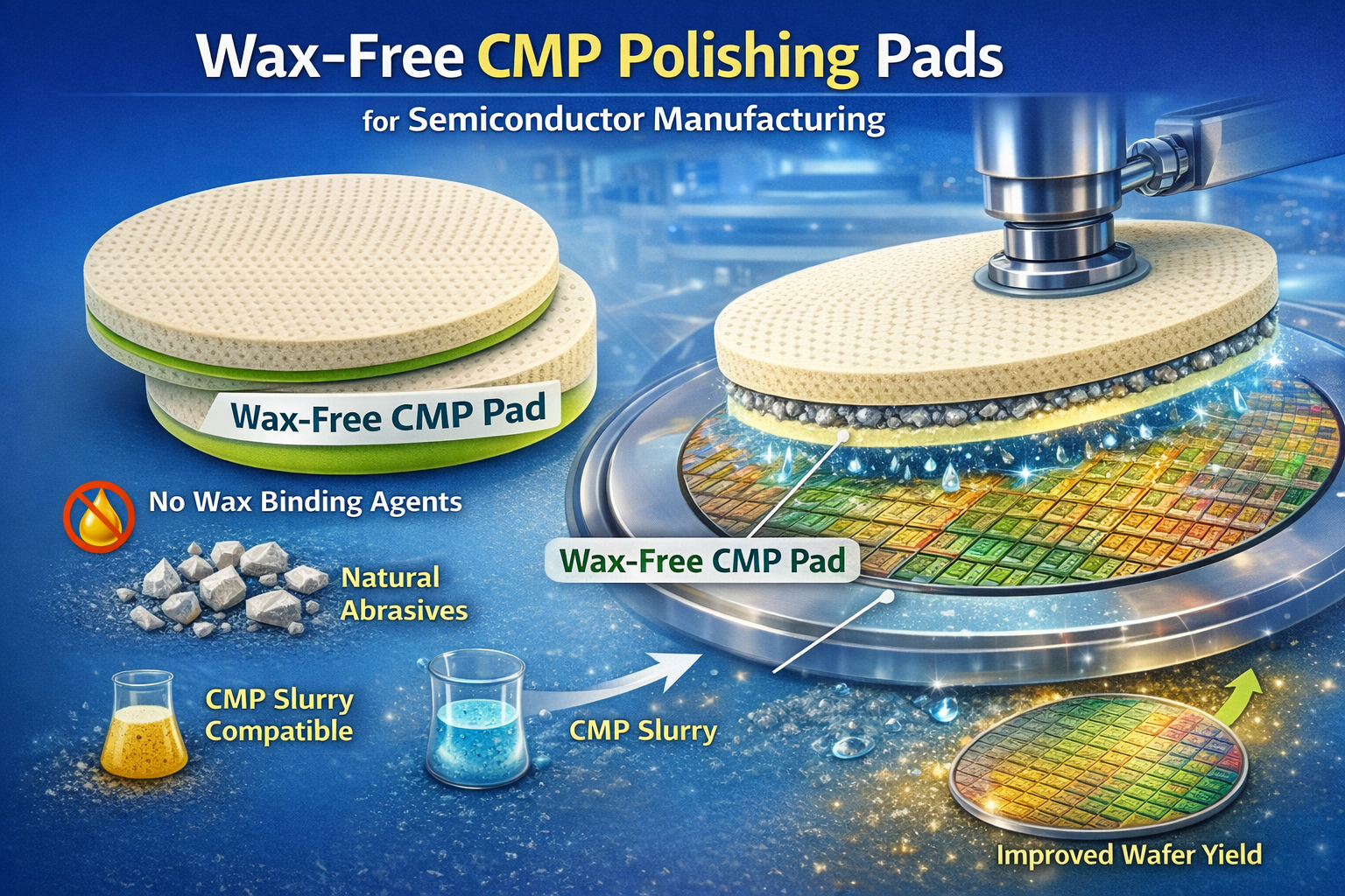
Explication des matériaux et de la structure des tampons de polissage CMP

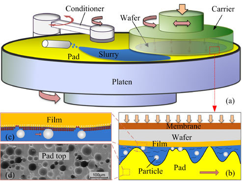
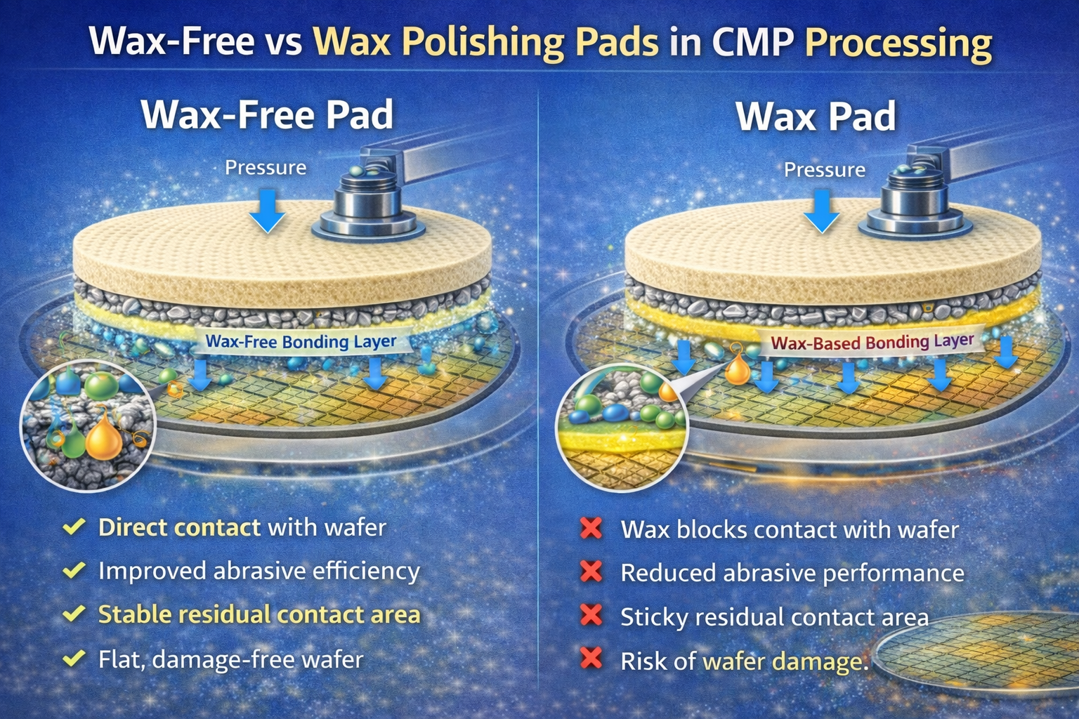
Dans le domaine du CMP, les matériaux des tampons de polissage définissent les interactions mécaniques, chimiques et tribologiques fondamentales qui déterminent en fin de compte l'efficacité de la planarisation, la défectuosité et la stabilité du processus. Pour les tampons de polissage CMP sans cire, la sélection des matériaux devient encore plus critique car la fixation de la plaquette, la transmission de la force et l'interaction de la boue sont régies directement par les propriétés de masse et de surface du tampon plutôt que par les couches de cire auxiliaires. Ce document fournit une analyse des matériaux des tampons de polissage CMP au niveau des matériaux et des mécanismes, en se concentrant sur les systèmes de polymères, la conception microstructurale, les paramètres mécaniques, le comportement à l'usure et leurs implications spécifiques pour les architectures de tampons sans cire. Table des matières Vue d'ensemble des matériaux pour tampons de polissage CMP Chimie des polymères et conception de la matrice Microstructure et ...

Par |2026-01-12T10:54:52+08:002026年1月12日|Blog, L'industrie|0 Commentaires

Les tampons de polissage sans cire dans les applications du procédé CMP

Dans la fabrication moderne de semi-conducteurs, le CMP n'est plus une opération unitaire isolée, mais un module de processus étroitement intégré qui interagit avec le dépôt en amont, le nettoyage en aval et la gestion du rendement global. L'adoption de tampons de polissage CMP sans cire modifie fondamentalement la manière dont les plaquettes sont maintenues, chargées, polies et libérées, ce qui nécessite une intégration délibérée du processus plutôt qu'un simple remplacement des consommables. Ce document se concentre sur la manière dont les tampons de polissage sans cire sont pratiquement intégrés dans les processus CMP, sur les paramètres de processus qui sont directement affectés et sur la manière dont les usines peuvent tirer parti des architectures sans cire pour améliorer la stabilité du processus, la constance du rendement et la rentabilité. Table des matières Intégration des tampons sans cire dans les procédés CMP ...

Par |2026-01-12T10:53:59+08:002026年1月12日|Blog, L'industrie|0 Commentaires

Wax-Free vs Wax Polishing Pads in CMP Processing

In chemical mechanical planarization (CMP), the polishing pad is not merely a consumable surface but a critical process component that directly affects wafer flatness, material removal rate (MRR), defectivity, yield stability, and overall cost of ownership (CoO). Among available pad architectures, wax-free CMP polishing pads and traditional wax-based polishing pads represent two fundamentally different philosophies of wafer fixation, force transmission, and contamination control. This page provides an engineering-level comparison between wax-free and wax polishing pads, focusing on structural design, adsorption mechanisms, process behavior, defect risks, maintenance complexity, and long-term manufacturing economics. The goal is to support data-driven decision-making rather than ...

Par |2026-01-12T10:49:50+08:002026年1月12日|Blog, L'industrie|0 Commentaires

Comment les tampons de polissage sans cire fonctionnent-ils dans les processus CMP ?

    Table of Contents 1. Introduction: Why Wax-Free Pad Working Principles Matter 2. CMP System Context: Wax-Free Pads as a Mechanical Subsystem 3. Pad–Wafer Contact Mechanics Without Wax Bonding 4. Wafer Loading and Initial Adsorption Formation 5. Pressure Ramp-Up and Adsorption Force Stabilization 6. Slurry Introduction and Frontside–Backside Decoupling 7. Steady-State CMP: Dynamic Adsorption Under Motion 8. Thermal and Mechanical Stability During CMP Operation 9. Controlled Wafer Release and De-Adsorption Behavior 10. Manufacturing-Level Process Control Implications 1. Introduction: Why Wax-Free Pad Working Principles Matter Understanding how wax-free polishing pads work is essential for modern CMP process development because wafer ...

Par |2026-01-12T10:42:02+08:002026年1月12日|Blog, L'industrie|0 Commentaires

Technologie du tampon de polissage à adsorption sans cire

  Table of Contents 1. Technology Overview: Adsorption as a Replacement for Wax Bonding 2. Fundamental Sources of Adsorption Force in Wax-Free Pads 3. Pad Microstructure Design and Adsorption Efficiency 4. Contact Mechanics at the Pad–Wafer Interface 5. Tunable Engineering Parameters Affecting Adsorption 6. Adsorption Stability Under CMP Operating Conditions 7. Adsorption Degradation and Failure Modes 8. Position of Adsorption Technology Within CMP Systems 1. Technology Overview: Adsorption as a Replacement for Wax Bonding Wax-free adsorption polishing pad technology was developed to eliminate the inherent limitations of wax-based wafer bonding in CMP. Traditional wax layers introduce viscoelastic behavior, thermal sensitivity, ...

Par |2026-01-12T10:48:33+08:002026年1月12日|Blog, L'industrie|0 Commentaires

Pads de polissage CMP sans cire pour la fabrication de semi-conducteurs

  Table of Contents 1. Definition and Technical Scope of Wax-Free CMP Polishing Pads 2. Product Forms and Design Intent of Wax-Free Polishing Pads 3. Core Technology: Wax-Free Adsorption Fundamentals 4. How Wax-Free CMP Polishing Pads Work in Practice 5. Wax-Free vs Wax-Based CMP Polishing Pads 6. Integration of Wax-Free Pads in CMP Processes 7. Material and Structural Foundations of Wax-Free CMP Pads 1. Definition and Technical Scope of Wax-Free CMP Polishing Pads Wax-free CMP polishing pads are engineered wafer holding and polishing interfaces designed to operate without wax or adhesive bonding layers during chemical mechanical planarization. Unlike traditional wax-based ...

Par |2026-01-12T10:46:47+08:002026年1月12日|Blog, L'industrie|0 Commentaires

How to Choose CMP Slurry

  An Engineering-Level Decision Framework for Semiconductor Wafer Polishing Table of Contents 1. Introduction 2. First-Principles Approach to Slurry Selection 3. Wafer Material Considerations 4. Matching Slurry Type to CMP Process 5. Key Performance Metrics 6. Process Window & Margin Engineering 7. Compatibility with CMP Polishing Pads 8. Defectivity & Yield Risk Assessment 9. CMP Tool & Delivery System Constraints 10. High-Volume Manufacturing (HVM) Considerations 11. Common CMP Slurry Selection Mistakes 12. Qualification & Ramp-Up Strategy 13. Engineering Summary 1. Introduction Choosing the right CMP slurry is one of the most consequential decisions in semiconductor manufacturing. Unlike many consumables, slurry ...

Par |2026-01-05T16:34:14+08:002026年1月5日|Blog, L'industrie|0 Commentaires

CMP Slurry Filters

  Filter Media, Housing Design, and Point-of-Use Control in Semiconductor CMP Table of Contents 1. Overview of CMP Slurry Filters 2. Role of Filters in CMP Yield Control 3. Filter Media Materials 4. Absolute vs Nominal Rating 5. Pore Size Distribution & Cutoff Behavior 6. Filter Housing Design 7. Point-of-Use (POU) Filtration 8. Chemical Compatibility & Extractables 9. Performance Data & Lifetime Modeling 10. Failure Modes & Root Cause Analysis 11. HVM Filter Management Strategy 12. How to Select CMP Slurry Filters 13. Future Trends 1. Overview of CMP Slurry Filters CMP slurry filters are precision components designed to remove ...

Par |2026-01-05T16:28:13+08:002026年1月5日|Blog, L'industrie|0 Commentaires

CMP Slurry Filtration

  Particle Control, Yield Protection, and Process Stability in Semiconductor CMP Table of Contents 1. Introduction 2. Why Filtration Is Critical in CMP 3. Particle Sources in CMP Slurry Systems 4. Particle Size vs Defect Mechanisms 5. CMP Slurry Filter Technologies 6. Filter Pore Size Selection Strategy 7. Chemical Compatibility & Slurry Stability 8. Experimental Data & Filtration Performance 9. Filtration Process Window 10. Integration with CMP Tools 11. Filtration Failure Modes & RCA 12. HVM Filtration Strategy 13. Future Trends 1. Introduction CMP slurry filtration is one of the most underestimated yet yield-critical elements in semiconductor manufacturing. While slurry ...

Par |2026-01-05T16:25:16+08:002026年1月5日|Blog, L'industrie|0 Commentaires

Tungsten CMP Slurry for Semiconductor Manufacturing

  Table of Contents 1. Introduction to Tungsten CMP 2. Tungsten CMP Applications in Semiconductor Devices 3. Material Properties of Tungsten Relevant to CMP 4. Chemical–Mechanical Removal Mechanism 5. Tungsten CMP Slurry Composition Architecture 6. Chemical Kinetics & Rate-Limiting Steps 7. Engineering Parameters & Experimental Data 8. Process Window & Control Maps 9. Defect Mechanisms & Root Cause Analysis 10. High-Volume Manufacturing Challenges 11. Slurry Selection & Optimization Guidelines 12. Future Trends in Tungsten CMP Slurry 1. Introduction to Tungsten CMP Tungsten Chemical Mechanical Planarization (CMP) plays a critical role in semiconductor manufacturing, particularly for contact plug and via fill ...

Par |2026-01-05T16:19:16+08:002026年1月5日|Blog, L'industrie|0 Commentaires
Haut de page