Wafer Dicing Blade Specifications: Dimensions & Parameters — Complete Reference
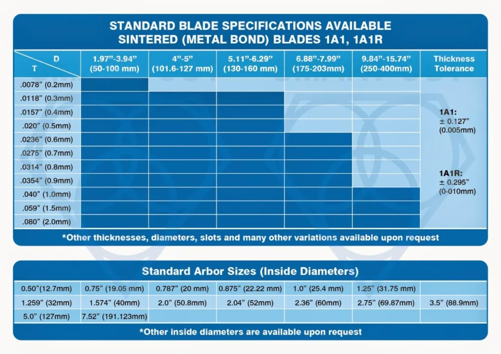
Technical Reference · May 2026 A comprehensive technical reference covering all standard dimensional parameters for wafer dicing blades — outer diameter, inner diameter, blade thickness, exposure, grit size, concentration, and ...


