logo

semiconductorについて

この著者はまだ詳細を記入していない。.
これまでsemiconductorは51のブログエントリーを作成した。.

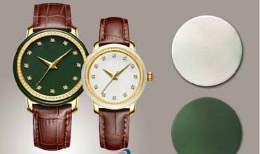
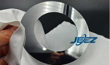
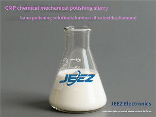
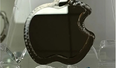
金属研磨スラリー-アップルロゴ鏡面研磨スラリー

アップルのロゴは、鏡のようにきらきらと輝き、アップル・ブランドの魅力と美学を表現しています。完璧なアップルロゴを作るには、化学機械研磨(CMP)技術による研磨が必要です。CMPプロセスは、より高い表面平滑性と安定した効率を実現し、高い歩留まり率を保証すると同時に、より良いブランドイメージを構築します。アップルのロゴは、6063アルミニウム合金またはステンレススチール製です。まずCNCでロゴの形にカットされ、次に表面研磨機で研磨されます。粗研磨とレベリングには、複合粗研磨パッドとCMP研磨スラリーが使用されます。.

|2025-12-16T11:39:06+08:002025年12月9日|申し込み|0 コメント

翡翠研磨スラリー-CMPによる翡翠時計の文字盤研磨プロセス

顧客がデザインした翡翠の腕時計は、翡翠の高貴な個性を体現し、優雅で洗練された雰囲気を醸し出している。ヘティアン翡翠の文字盤の粗面除去と研磨は、CMP(化学機械研磨)技術によって達成される。GizhilエレクトロニクスのCMP研磨スラリーと研磨パッドを併用することで、原料表面の不均一な傷が除去され、翡翠の自然な光沢と固有の質感がよみがえります。研磨後のダイヤルワークは、緻密で滑らかで、蝋のような、油のような質感を示す。翡翠の研磨にCMPを使用する利点には、迅速な減厚、高い研磨効率、卓越した輝度、最小限の...

|2025-12-16T11:39:26+08:002025年12月9日|申し込み|0 コメント

半導体研磨スラリー-セラミック銅張基板 DPC研磨スラリー/DBC研磨液

Gizhil Electronic's ceramic copper-clad substrate grinding fluid / DPC polishing slurry / DBC grinding fluid typically involves two processes: coarse polishing and fine polishing. Depending on the customer's requirements for workpiece polishing and surface roughness, different DPC grinding fluids or fine polishing slurries are selected. The coarse polishing process for ceramic copper-clad DPC/DBC substrates primarily focuses on rapid thickness reduction and improved polishing efficiency. For DPC substrates requiring higher quality, a secondary fine polishing step is necessary to remove surface defects and imperfections. After using Gizhil Electronic's ceramic copper-clad substrate grinding fluid / fine polishing slurry, the surface roughness (Ra) ...

|2025-12-16T11:39:57+08:002025年12月9日|申し込み|0 コメント

金属研磨スラリー-CMPによる油圧部品リターンプレート/9ホールプレートの研磨

油圧システムの動力部品は、エンジンまたはモータによって駆動され、油圧タンクから油を吸入し、加圧された油を生成してアクチュエータに供給する。油圧ポンプは、構造によってギヤポンプ、ピストンポンプ、ベーンポンプ、スクリューポンプに分類される。油圧ポンプの付属品には、ポートプレート、リターンプレート、可変ヘッド、ドライブシャフト、ピストンスリッパなどがあります。これらの油圧鋳物には、研磨パッドと研磨スラリーを使用して、バリや切削痕のない平滑な金属表面を実現するCMP(化学的機械研磨)技術による加工が必要です。この工程は、部品組立後の摩耗を低減し、騒音を低減し、...

|2025-12-16T11:42:04+08:002025年12月9日|申し込み|0 コメント

サファイアウェハーの研削と研磨

サファイアウェーハを研磨する目的は、基板の最終的な厚さを所望の目標値まで薄くすることであり、±2μm以上のTTV(総厚さばらつき)と2nm以下の表面粗さを達成することである。このような動作要件には、高精度、高効率、安定性を備えた機械とプロセスが必要です。GizhilエレクトロニクスのCMP(化学的機械研磨)用サファイア研磨スラリーと研磨パッドを使用することで、この工程を実現することができる。CMP研磨技術を採用することで、サファイアワークは所望の表面粗さを達成することができる。各研磨サファイアウェハは、加工中に均一な材料除去を受け、...

|2025-12-16T11:42:41+08:002025年12月9日|申し込み|0 コメント

アルミニウム合金研磨スラリー-アルミニウム工作物の鏡面研磨

Aluminum alloy is relatively soft and has low hardness, making it highly susceptible to mechanical damage such as scratches and abrasions during processing, as well as corrosion and poor chemical stability on the surface. To eliminate defects from the machining process, the CMP (Chemical Mechanical Polishing) method is commonly employed to achieve excellent surface smoothness. With the advancement of high-tech processes, Gizhil Electronic's aluminum alloy polishing slurry now offers mature technical support, enabling ultra-precise and nearly defect-free planarization of CMP-polished materials. CMP truly achieves global planarization of aluminum alloy substrates, delivering near-perfect surfaces with extremely low roughness while significantly improving ...

|2025-12-16T11:43:07+08:002025年12月9日|申し込み|0 コメント

炭化ケイ素ウェハー研磨スラリー

Gizhil Electronic's silicon carbide fine polishing slurry is suitable for the surface planarization of SiC silicon carbide wafer substrates during precision machining. The slurry used for wafer polishing exhibits high polishing efficiency and low surface roughness. After polishing with Gizhil Electronic's SiC substrate polishing slurry, the wafer surface is free from defects such as scratches and haze, ensuring excellent flatness of the silicon carbide wafers. Developed by Gizhil Electronic, this silicon carbide polishing slurry offers a high dilution ratio and easy post-polishing cleaning, making it widely applicable in the manufacturing of semiconductor integrated circuit substrates. Gizhil Electronic's SiC slurry for ...

|2025-12-16T11:43:32+08:002025年12月9日|申し込み|0 コメント

硬質合金研磨スラリー-タングステン鋼ブレードの鏡面研磨

硬質合金ブレードは、高硬度、良好な靭性、耐熱性、耐食性など、一連の優れた特性を持っている。特に、その高い硬度と耐摩耗性により、1000℃でもかなりの硬度を維持することができます。硬質合金で作られたタングステン鋼のワークは、多くの研磨プロセスのための挑戦的な材料と見なされます。現在、タングステン鋼ブレードは、理想的な表面仕上げを達成するために、特殊な金属研磨スラリーと組み合わせたCMP(化学機械研磨)技術を使用して研磨することができます。タングステン鋼ブレードとして知られている硬質合金ブレードは、多くの場合、生のワークピース上の錆スポット、傷、孔食などの表面欠陥を示す。 ...

|2025-12-16T11:43:53+08:002025年12月9日|申し込み|0 コメント

炭化ケイ素(SiC)研磨プロセス

CMP(化学的機械研磨)スラリーは、半導体産業の特定のプロセスに応じて、誘電体層CMPスラリー、バリア層CMPスラリー、銅CMPスラリー、シリコンCMPスラリー、タングステンCMPスラリー、TSV(Through-Silicon Via)CMPスラリー、シャロートレンチ・アイソレーションCMPスラリーなどに分類されます。SiC CMPスラリーは、半導体ウェハー製造工程で必要不可欠な材料の一つです。炭化ケイ素材料のワークピースの研磨において重要な役割を果たします。スラリーの種類、粒子分散、粒子径、物理化学的特性、安定性などの要因は、研磨結果に密接に関係しています。近年、...

|2025-12-16T11:44:19+08:002025年12月9日|申し込み|0 コメント

Analysis of Key Polishing and Lapping Processes for InP (Indium Phosphide) Substrates

Indium Phosphide (InP), as a core material of the third-generation semiconductor, holds an irreplaceable position in high-end fields such as optical communications, millimeter-wave radar, and quantum communications due to its excellent electron mobility, wide bandgap, and superior optoelectronic properties. The surface quality of InP substrates directly determines the precision and reliability of subsequent epitaxial growth and device fabrication, with polishing and lapping processes being the critical steps in controlling this core metric. Drawing on years of practical experience in semiconductor material processing, Gizhi Electronics provides a systematic analysis of the key polishing and lapping processes for InP substrates, along with ...

|2025-12-25T10:48:50+08:002025年12月5日|ブログ, 産業|0 コメント
このページのトップへ