随时了解集智电子的最新发展、重要公告和企业新闻。我们致力于与客户分享公司的成长历程和重要里程碑。.
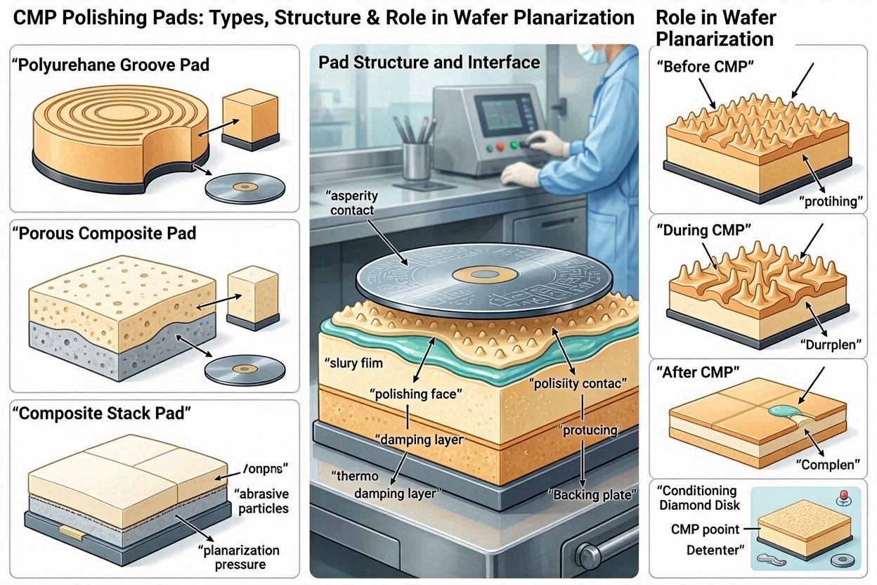
← Back to Complete Planarization Guide CMP Consumables — Polishing Pads The CMP polishing pad is the mechanical foundation of the planarization process. Its hardness, porosity, groove geometry, and surface ...
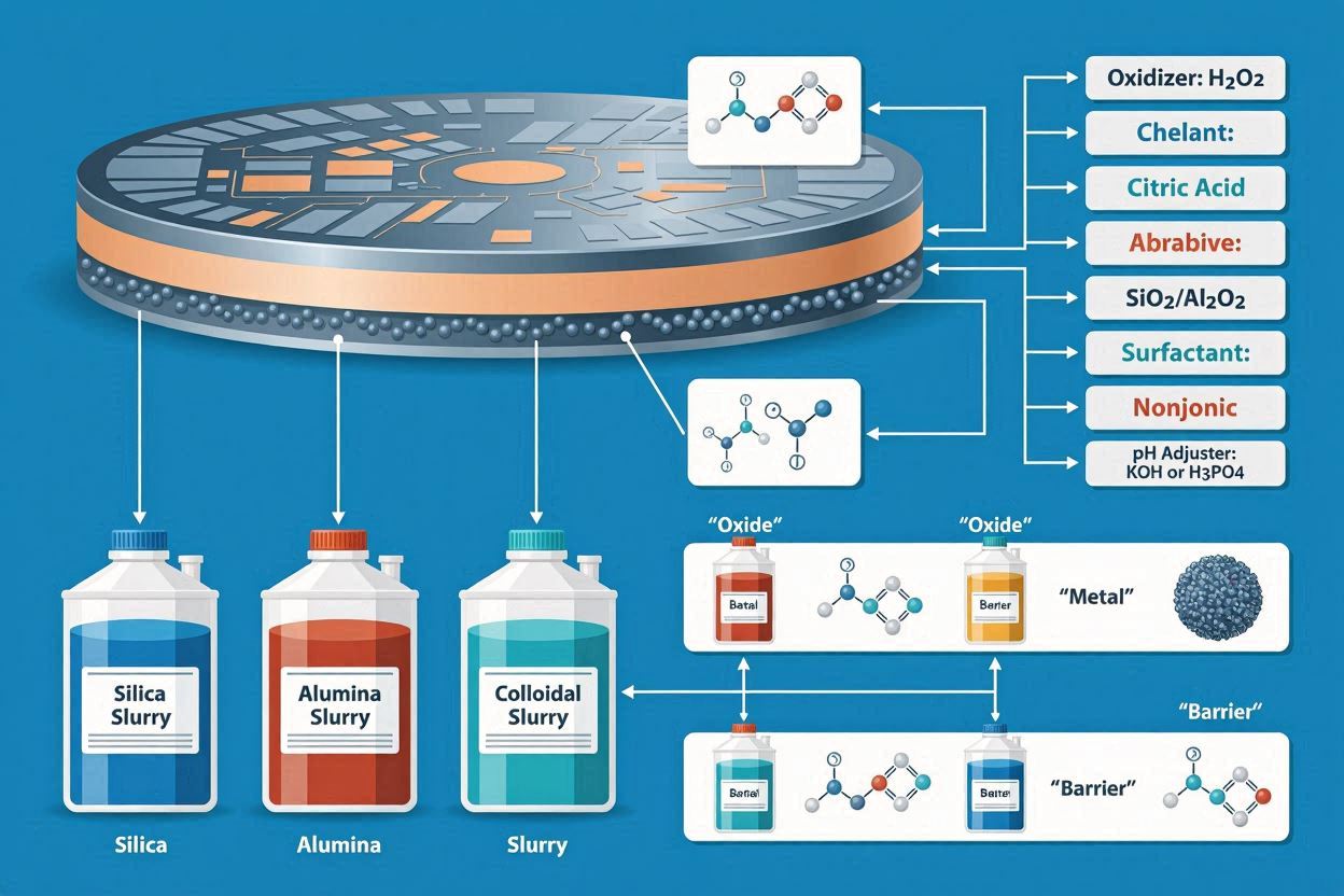
← Back to Complete Planarization Guide CMP Consumables — Slurry CMP slurry is the active medium through which both material removal and surface quality are determined in semiconductor planarization. This ...
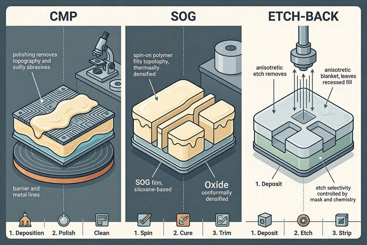
← Back to Complete Planarization Guide Process Technology Comparison Semiconductor planarization encompasses a range of techniques that have evolved over six decades — from thermal glass reflow and spin-on-glass to ...
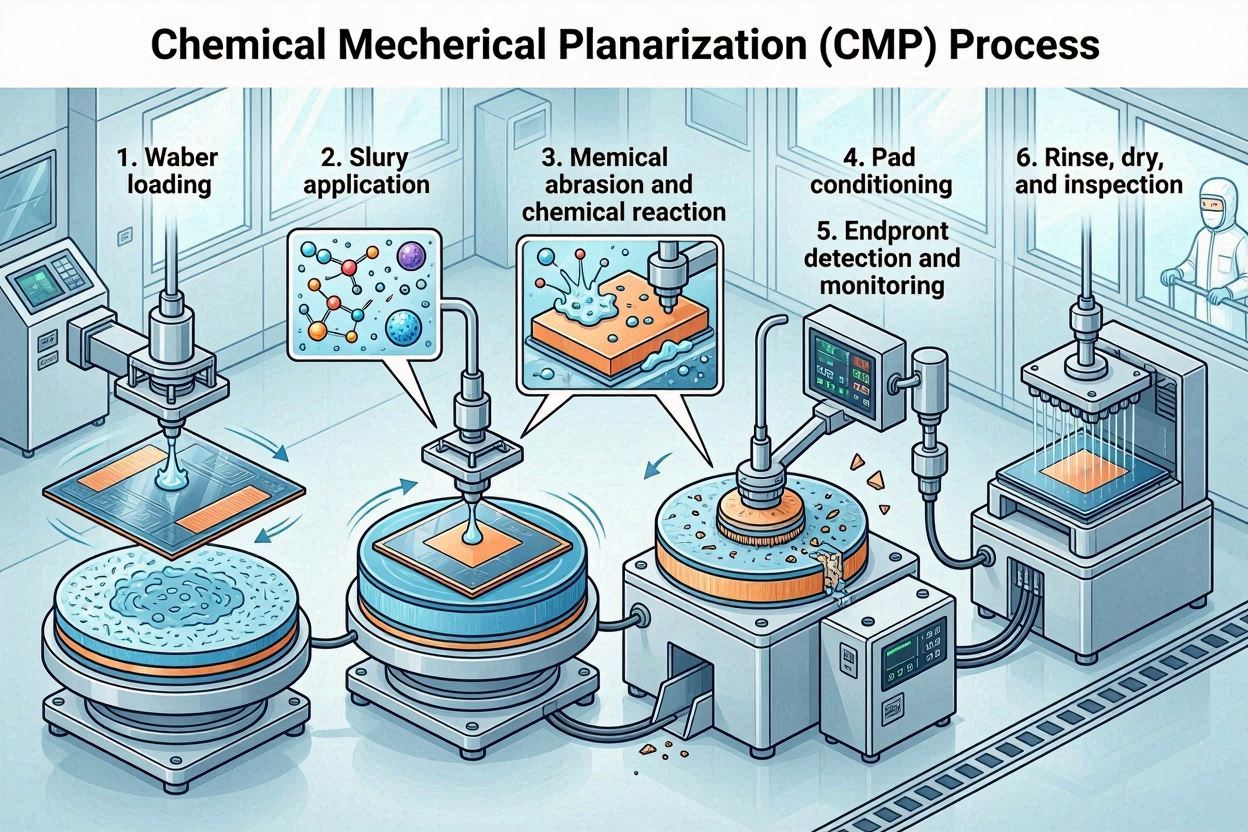
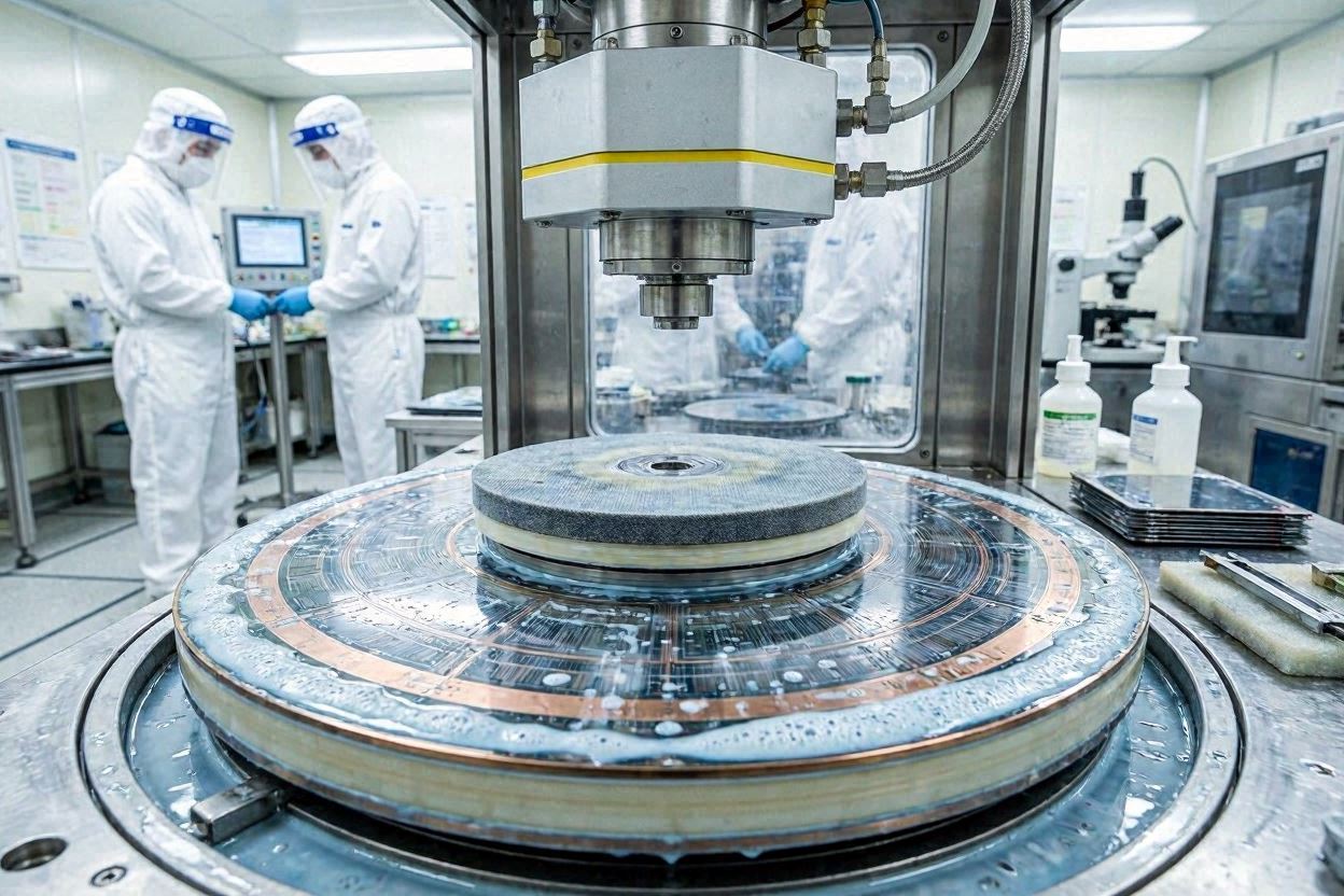
← Back to Complete Planarization Guide CMP Process Engineering Chemical Mechanical Planarization combines chemical reactivity and mechanical abrasion to remove material from wafer surfaces and achieve global planarization. This guide ...
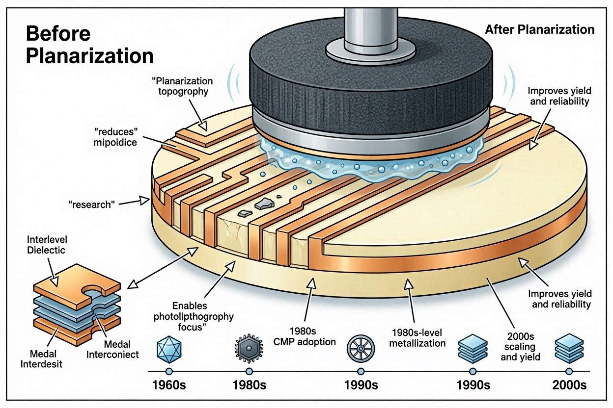
← Back to Complete Planarization Guide Semiconductor Fundamentals Semiconductor planarization is the process of reducing or eliminating surface topography on a wafer during integrated circuit fabrication. This article covers the ...
Semiconductor Process Technology Semiconductor planarization is one of the most process-critical techniques in modern chip fabrication. Without it, every layer added to a wafer would inherit and amplify the topographic ...
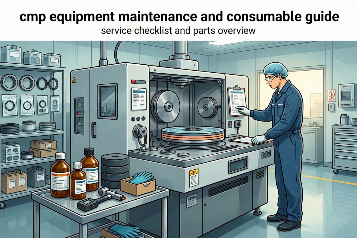
This article is part of our complete guide to chemical mechanical planarization equipment. Consistent CMP performance depends as much on disciplined consumable management and preventive maintenance as it does on ...

This article is part of our complete guide to chemical mechanical planarization equipment. Choosing a CMP equipment supplier is a decision that shapes process capability, consumable sourcing, and support quality ...
This article is part of our complete guide to chemical mechanical planarization equipment. As process nodes shrink and chip designs increasingly rely on advanced packaging, CMP equipment is being asked ...
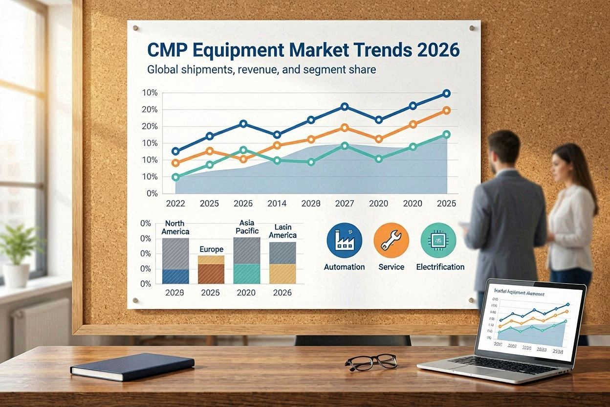
This article is part of our complete guide to chemical mechanical planarization equipment. Understanding where the CMP equipment market is heading — and why — helps fab managers, process engineers, ...
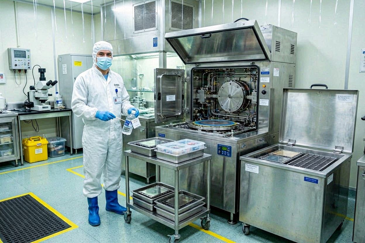
This article is part of our complete guide to chemical mechanical planarization equipment. Polishing is only half of the CMP story — what happens immediately afterward, in the cleaning modules, ...
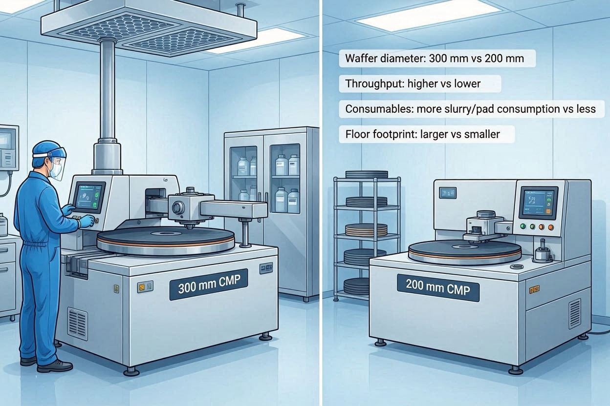
This article is part of our complete guide to chemical mechanical planarization equipment. Wafer size has a bigger impact on CMP equipment design than it might first appear — affecting ...