炭化ケイ素(SiC)研磨プロセス
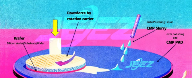
CMP(化学的機械研磨)スラリーは、半導体産業のプロセスに応じて、誘電体層CMPスラリー、バリア層CMPスラリー、銅CMPスラリー、シリコンCMPスラリー、...に分類することができます。.
CMP(化学的機械研磨)スラリーは、半導体産業のプロセスに応じて、誘電体層CMPスラリー、バリア層CMPスラリー、銅CMPスラリー、シリコンCMPスラリー、...に分類することができます。.
Indium Phosphide (InP), as a core material of the third-generation semiconductor, holds an irreplaceable position in high-end fields such as optical communications, millimeter-wave radar, and quantum communications due to its ...
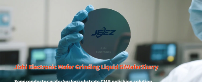
In the precision manufacturing chain of the semiconductor industry, the creation of every high-performance chip relies on hundreds of process steps, from silicon purification to chip packaging. Among these, silicon ...
As the third-generation semiconductor industry accelerates its iteration today, silicon carbide (SiC), as a core material, is reshaping the technological landscape of high-end manufacturing fields such as new energy vehicle ...
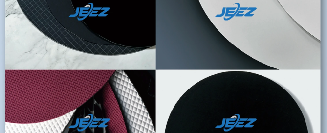
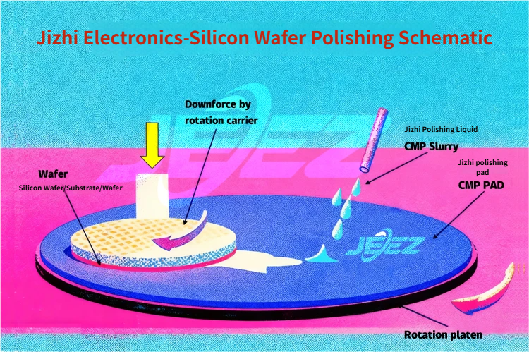
Unlocking CMP Process: Principles and Advantages In the field of optical component processing, Chemical Mechanical Polishing (CMP) is a core technology for achieving high-precision surface planarization. Through the synergistic effects ...
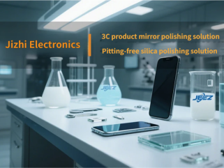
Why Choose CMP Over Electrochemical Polishing for 3C Product Mirror Polishing? In the 3C industry (mobile phones, laptops, smart wearables, etc.), electrochemical polishing is gradually being replaced by CMP (Chemical ...
In fields such as semiconductor manufacturing, precision optics, and hard alloy processing, the ultra-precision polishing of material surfaces directly determines product performance and reliability. Leveraging advanced R&D capabilities and mature ...
I. CMP Polishing Technology: A Key Process in Semiconductor Manufacturing Chemical Mechanical Planarization (CMP) is one of the core processes in semiconductor silicon wafer manufacturing, directly impacting chip performance and ...
In the global planarization stage of wafer manufacturing, Chemical Mechanical Polishing (CMP) is a critical process. As a core consumable, CMP polishing slurry directly determines key wafer surface metrics such ...
Polishing the stainless steel back cover of a smart watch requires both the rough and fine polishing stages of the CMP process. Using Jizhi Electronics' polishing slurry and pads in ...

高精度表面処理材料
ポリッシングスラリー - ポリッシングパッド - 半導体用ダイシングブレード
重要な製造工程における信頼性と一貫性。.
著作権 ©2026 無錫吉芝電子科技有限公司.

電話
+(86) 180-6835-1533

電子メール
contact@jeez-semicon.com

住所
中国江蘇省無錫市