

FAスラリー
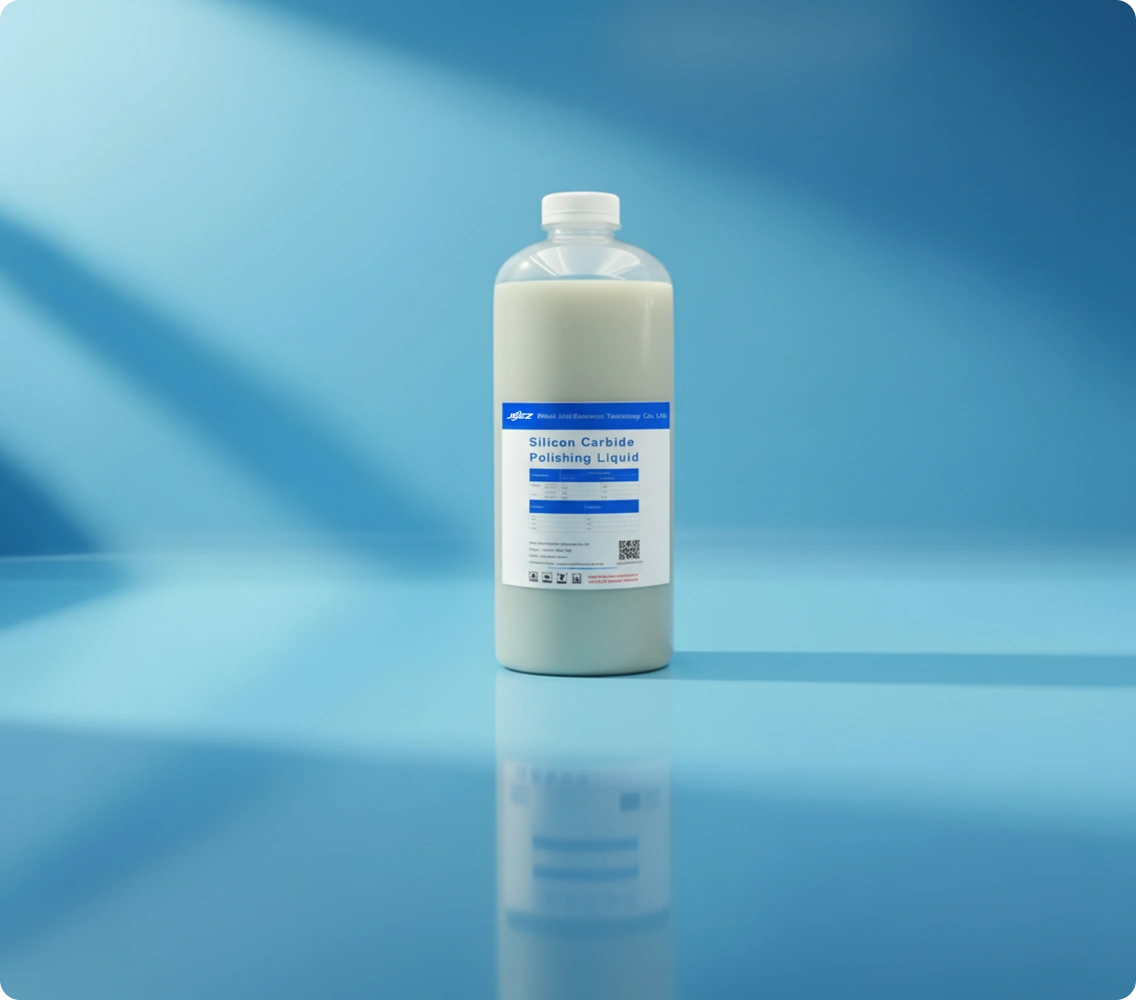
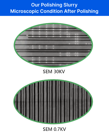
Suitable for FA/SEM/TEM analysis, meeting the requirements for ultra-fine surface finish.
Its special formulation supports final polishing of various materials, achieving an excellent mirror-like finish, particularly on non-ferrous metals, printed circuit boards, and integrated circuits.
主な特徴
- Removes cured polymer mixtures, soft hydrogels, nanoimprint materials, resist materials, etc. from glass substrates.
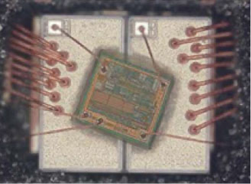
- Chip Defect Analysis
- Strips coatings from the substrate without scratching or residue, achieving an ideal surface condition.
製品名
Suitable for FA/SEM/TEM analysis, meeting the requirements for ultra-fine surface finish.
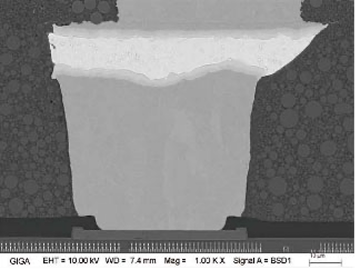
In the analysis of failure:
Polishing can be used to observe the surface details of products or materials to determine whether there are any defects or damages. For instance, surface cracks, fatigue cracks, corrosion, oxidation and other defects can be observed through polishing, thereby determining the cause of failure. Additionally, polishing can also be used to prepare samples for microscopic observation or other tests.
Overall, polishing is an important tool in failure analysis, which can help analysts better observe and understand the causes of product or material failure.
製品の特徴
In the CMP process for tungsten (W), there are two main application scenarios: one is its use as an interconnect between upper and lower layers, and the other is its use as a metal gate in advanced process technologies. In either case, the overall CMP process flow is essentially the same.
Tungsten CMP polishing slurry is primarily used for the CMP polishing of metal tungsten (W) to achieve precise surface planarity and thickness control. Semiconductor W CMP slurry typically contains chemical components such as oxidizers, acids, bases, and abrasives. The combination of these chemicals and abrasives provides high selectivity and low surface roughness during polishing. In semiconductor manufacturing, W CMP slurry is widely used in the fabrication of tungsten structures, including tungsten interconnects and metal gates.
Suitable for FA/SEM/TEM analysis, meeting the requirements for ultra-fine surface finish. Its special formulation supports final polishing of various materials, achieving an excellent mirror-like finish, particularly on non-ferrous metals, printed circuit boards, and integrated circuits.
Polish:
Localized or global grinding can be performed. Combined with ion milling, this provides a much clearer cross-sectional profile.
Decap:
Applicable to gold wire, copper wire, copper-plated wire, silver wire, and various package types, including ultra-small packages.
Delayer:
By using RIE with plasma gases such as O₂, CF₄, CHF₃, and SF₆, materials including oxides, nitrides, polyimide, and silicon can be removed. In combination with mechanical grinding, this enables layer-by-layer removal for advanced-node chips and BSI samples.
| Product Inspection Report | ||
| JZ-055 | ||
| Test Items | Test Method | Measured Value |
|---|---|---|
| Particle Size (nm) | Laser Particle Size Analyzer | 80 |
| Particle Size (nm) | pH Meter | 10.3 |
| Particle Size (nm) | Viscometer | 2.86 |
| Density (g/mL) | Densitometer | 1.254 |
| Nitrogen Content (ppm) | UV Spectrophotometer | 7.09 |
| Our products can be used as substitutes for foreign brands such as Axxd and Bxxxxr. | ||
Storage Method for JIZHI Electronics FA Slurry
換気の良い、涼しく乾燥した倉庫で保管すること。製品は直射日光と凍結を避け、5~35℃で保管すること。0 °C以下で保管すると、不可逆的な凝集が起こり、製品が使用できなくなることがある。.
JIZHIエレクトロニクスCMP/スラリー研磨液の価格
JIZHIエレクトロニクスのCMP用金属研磨スラリーは、海外の高度な生産技術と設備により製造され、特殊な化学組成で調合されています。輸入品と比較しても遜色のない品質です。.
現地生産により、JIZHIエレクトロニクスのCMPスラリーは、短納期、安定した高品質、競争力のある費用対効果の高い価格設定を実現しています。.
Jizhi Electronicsを選ぶ理由
光学材料CMPにおける10年の経験
光学材料CMPにおける10年の経験
研磨液と処方は柔軟にカスタマイズ可能
国際規格に適合した無害で生分解性の処方
フリー・プロセス・デバッグ
40%従来品より処理時間を短縮
海外生産技術・設備の導入
最適化された消費率により、全体的な稼働率を低減