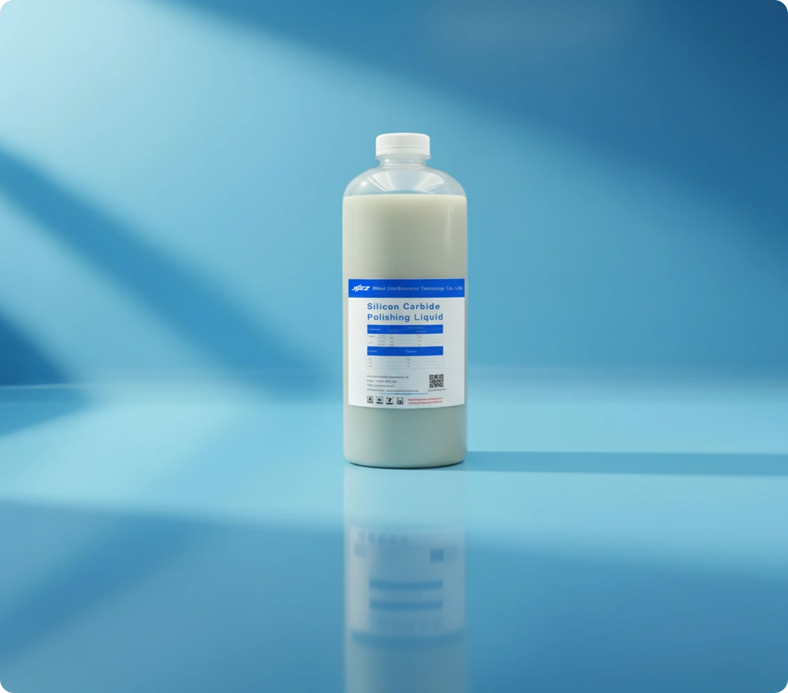


Indium Phosphide (InP) Polishing Slurry
Indium Phosphide (InP) polishing slurry / CMP slurry formulation tailored for the semiconductor and optical industries
Indium Phosphide (InP) Wafer Polishing Slurry / InP Polishing Slurry
主な特徴
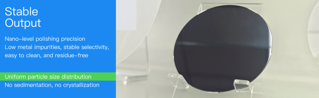
- High-purity raw materials with no contamination
- Fast polishing rate with high planarization
- High removal rate, good stability, low damage layer, and excellent surface quality
製品名
Indium Phosphide (InP) polishing slurry / CMP slurry formulation tailored for the semiconductor and optical industries
Product Description
Indium Phosphide (InP) polishing slurry / CMP slurry formulation tailored for the semiconductor and optical industries, suitable for planarization processing of InP wafers. Designed to meet the requirements of all process stages from grinding to CMP in substrate manufacturing, it provides a high-performance and cost-effective solution for InP wafer polishing applications.
製品の特徴
High-purity raw materials with no contamination
Fast polishing rate with high planarization
High removal rate, good stability, low damage layer, and excellent surface quality
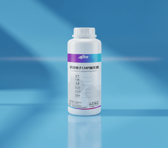
Features of JIZHI Electronics CMP Indium Phosphide (InP) Grinding/Polishing Slurry
1.The formulation is designed to meet the requirements of all process stages from grinding to CMP in substrate manufacturing, enabling rapid thinning and polishing of InP wafers.
2.Achieves high removal rates on InP surfaces with no subsurface damage, while providing excellent stability and reusability.
3.JIZHI Electronics sapphire slurry combinations offer high performance and cost-effective solutions.
4.Customized 1-to-1 solutions can be provided according to specific grinding and polishing requirements.
Material Properties and Application Value of InP
Core Material Properties
Indium phosphide, as an important semiconductor material, features high electron mobility and a wide bandgap, making it a key foundational material for optoelectronic and high-frequency devices.
Main Application Fields
It is widely used in optoelectronics and communication fields, with irreplaceable applications in optical communication devices, infrared detectors, and high-frequency transistors.
Importance of Polishing Process
The polishing process directly affects the surface quality and performance of indium phosphide materials, making it a critical step in improving application reliability and device performance.
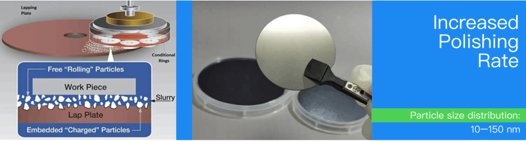
Indium Phosphide (InP) Polishing Process Parameters
InP CMP Polishing Process Parameters
| InP CMP Polishing Process Parameters | |
|---|---|
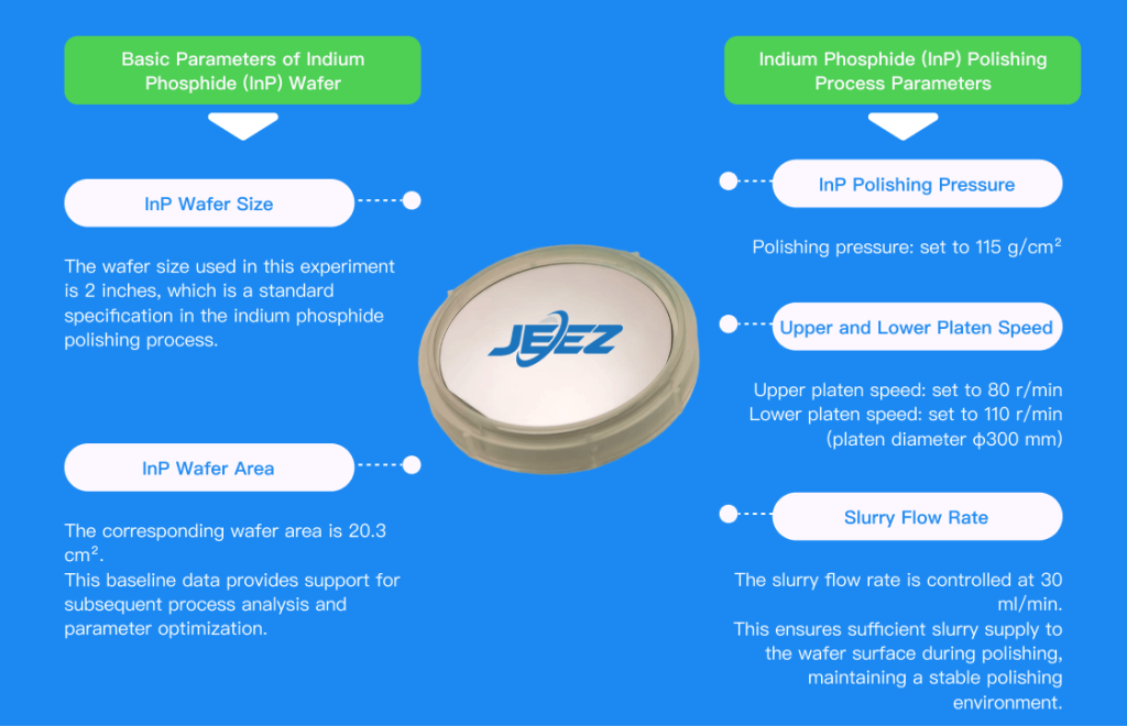
| Wafer Size (inch) | 2 |
| Wafer Area (cm²) | 20.3 |
| Polishing Pressure (g/cm²) | 115 |
| Upper Platen Speed (r/min) | 80 |
| Lower Platen Speed (r/min)(Platen Diameter φ300 mm) | 110 |
| Slurry Flow Rate (ml/min) | 30 |
| InP Wafer Post-Polishing Cleaning Process |
Immediately rinse the wafer with deionized water after unloading to keep the surface wet. Rinse the wafer surface and polishing carrier evenly with deionized water for 1 minute. After rinsing, dry the wafer using high-purity nitrogen or a spin dryer. |
Experimental Data Comparison
| Experimental Data | Finished Standard Wafer | Japanese F Competitor Slurry | JIZHI Self-Developed Slurry (F-System Equivalent) |
|---|---|---|---|
| Slurry pH Value | / | 3.2 | 2.9 |
| Removal Rate (μm/min) | / | 0.21 | 0.33 |
| Surface Roughness (nm) | <0.2 | 0.2 | 0.19 |
| Usage Method | Purchased standard wafer (sample) | 1 g powder + 500 g water + 180 g polishing slurry | 1 g powder + 500 g water + 125 g polishing slurry |
JIZHIエレクトロニクスSiC炭化ケイ素研磨スラリーの保管方法
換気の良い、涼しく乾燥した倉庫で保管すること。製品は直射日光と凍結を避け、5~35℃で保管すること。0 °C以下で保管すると、不可逆的な凝集が起こり、製品が使用できなくなることがある。.
JIZHIエレクトロニクスCMP/スラリー研磨液の価格
JIZHIエレクトロニクスのCMP用金属研磨スラリーは、海外の高度な生産技術と設備により製造され、特殊な化学組成で調合されています。輸入品と比較しても遜色のない品質です。.
現地生産により、JIZHIエレクトロニクスのCMPスラリーは、短納期、安定した高品質、競争力のある費用対効果の高い価格設定を実現しています。.
Jizhi Electronicsを選ぶ理由
光学材料CMPにおける10年の経験
光学材料CMPにおける10年の経験
研磨液と処方は柔軟にカスタマイズ可能
国際規格に適合した無害で生分解性の処方
フリー・プロセス・デバッグ
40%従来品より処理時間を短縮
海外生産技術・設備の導入
最適化された消費率により、全体的な稼働率を低減