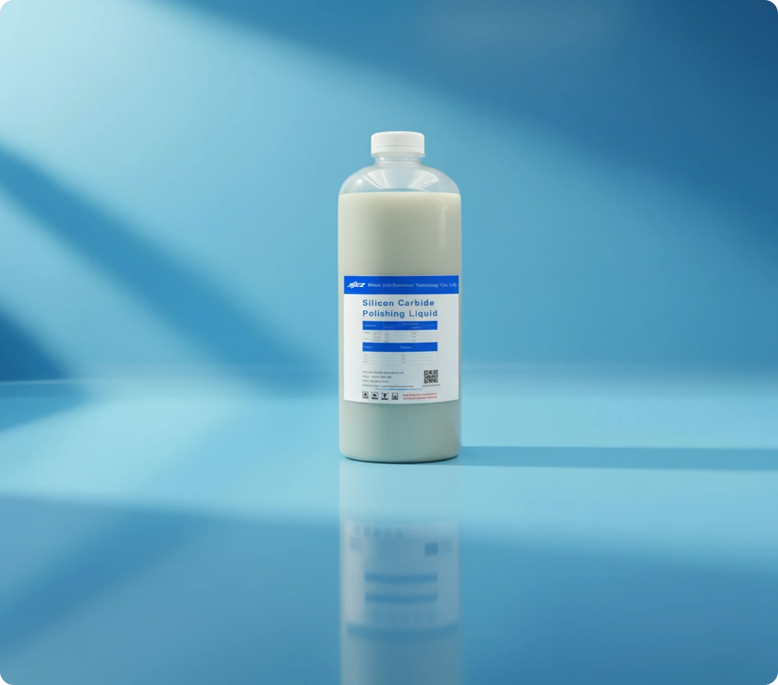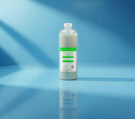


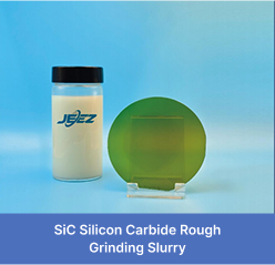
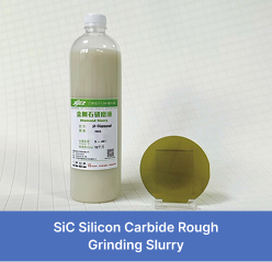
Silicon Carbide Substrate Grinding Slurry
JIZHI Electronics · Silicon Carbide Grinding and Polishing · Semiconductor Wafer Polishing
Silicon Carbide Grinding Slurry / Silicon Carbide Polishing Slurry / Silicon Carbide (SiC) Lapping Pad / SiC Final Polishing Pad
主要功能
- Domestic Alternatives to Politex and FUJIBO Polishing Pads
产品名称
JIZHI Electronics · Silicon Carbide Grinding and Polishing · Semiconductor Wafer Polishing
产品类别
JIZHI Electronics – Silicon Carbide Grinding / Semiconductor Wafer Polishing
产品特点
JIZHI Electronics provides two-stage polishing process solutions for silicon carbide (SiC), combining different models of grinding slurries and polishing pads (rough grinding pad / fine grinding pad / rough polishing pad / fine polishing pad). This approach improves the surface quality of SiC substrates during grinding while significantly increasing the material removal rate.
Process and Applications
Suitable for DMP and CMP processes of SiC substrates, effectively improving efficiency and yield. SiC grinding slurries and polishing pads enable domestic substitution for imported products.
Brief Overview of the Silicon Carbide Substrate Processing Flow
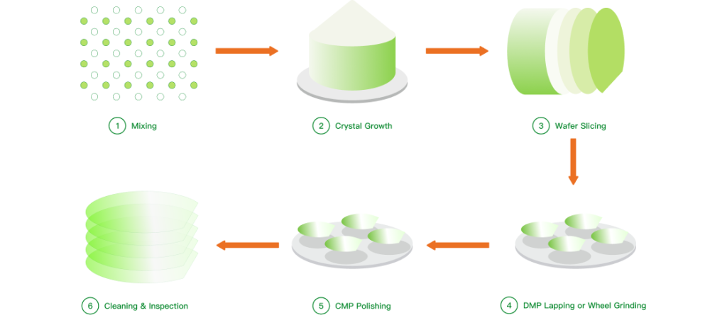
Silicon Carbide (SiC) Grinding Process – Rough Grinding / Fine Grinding
Step1
JIZHI Electronics Silicon Carbide (SiC) Rough Grinding Process
| SiC Double-Sided Rough Grinding Process | |
|---|---|
| Verification Equipment | double-sided36B |
| Wafer | 6″SiC |
| 抛光泥浆 | JZ-8003 |
| 抛光垫 | JZ-1020 |
| Pressure | 3 psi |
| Upper Platen Rotation Speed | 25 rpm |
| Lower Platen Rotation Speed | 10 rpm |
| Slurry Flow Rate | 5L /min |
| Polishing Rate | 25-30um/H |
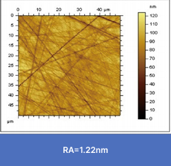
| Surface Roughness | 1.22nm |
| TTV (Total Thickness Variation) | <2 |
| Warp | <30 |
| Bow | <10 |
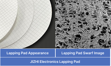
| Rough Grinding · Used with Lapping Pad | |
|---|---|
| Lapping Pad Dimensions and Specifications | |
| Model | JZ-1020 |
| 厚度 | 1.4 mm |
| Groove Pattern | 可定制 |
| 硬度 | Shore A 85° |
| 压缩比 | 2.92 |

Step2
JIZHI Electronics Silicon Carbide (SiC) Fine Grinding Process
| SiC Double-Sided Rough Grinding Process | |
|---|---|
| Verification Equipment | double-sided36B |
| Wafer | 6″SiC |
| 抛光泥浆 | JZ-8001 |
| 抛光垫 | JZ-1020 |
| Pressure | 3 psi |
| Upper Platen Rotation Speed | 25 rpm |
| Lower Platen Rotation Speed | 10 rpm |
| Slurry Flow Rate | 5L /min |
| Polishing Rate | 6.8um/H |
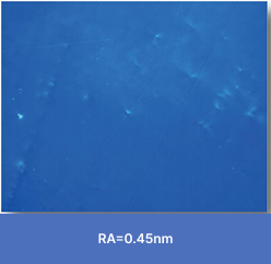
| Surface Roughness | 0.45nm |
| TTV (Total Thickness Variation) | <2 |
| Warp | <30 |
| Bow | <20 |
| ine Grinding · Used with Lapping Pad | |
|---|---|
| Lapping Pad Dimensions and Specifications | |
| Model | JZ-1020 |
| 厚度 | 1.4 mm |
| Groove Pattern | 可定制 |
| 硬度 | Shore A 85° |
| 压缩比 | 2.92 |
JIZHI Electronics’ CMP rough and fine grinding process for SiC substrates
Tip 1 – Using rough grinding slurry with a lapping pad, Ra can reach 1.22 nm or lower.
Tip 2 – Using fine grinding slurry with a lapping pad, Ra can reach 0.45 nm or lower.
Recommended Products and Parameters for Silicon Carbide Grinding / Polishing Processes
| Processing Method | Recommended Products | Removal Rate | Surface Quality | ||
|---|---|---|---|---|---|
| 抛光泥浆 | 抛光垫 | ||||
| Final Polishing | Grinding / Lapping | JZ-8003 | JZ-1020 | 25-30um/H | 1.22nm |
| Final Polishing | JZ-8001 | JZ-1020 | 6.8um/H | 0.45nm | |
Storage Method for JIZHI Electronics SiC Silicon Carbide Polishing Slurry
Store in a well-ventilated, cool, and dry warehouse. The product must be stored at 5–35 °C, protected from direct sunlight and from freezing. If stored below 0 °C, irreversible agglomeration may occur, rendering the product unusable.
Pricing of JIZHI Electronics CMP / Slurry Polishing Liquids
JIZHI Electronics’ CMP metal polishing slurries are manufactured using advanced overseas production technologies and equipment and are formulated with specialized chemical compositions. The quality of JIZHI Electronics’ polishing slurries is comparable to that of similar imported products.
Thanks to localized production, JIZHI Electronics’ CMP slurries offer short delivery lead times, stable high quality, and competitive, cost-effective pricing.
为什么选择集智电子?
10 年光学材料 CMP 经验
10 年光学材料 CMP 经验
抛光方案和配方可灵活定制
无毒、可生物降解配方,符合国际环保标准。
免费进程调试
40% 的处理时间比传统方法更快a
引进国外生产技术和设备
优化的消耗率降低了总体运行成本。